System Maintenance occurs every Friday.
System Maintenance occurs every Friday.
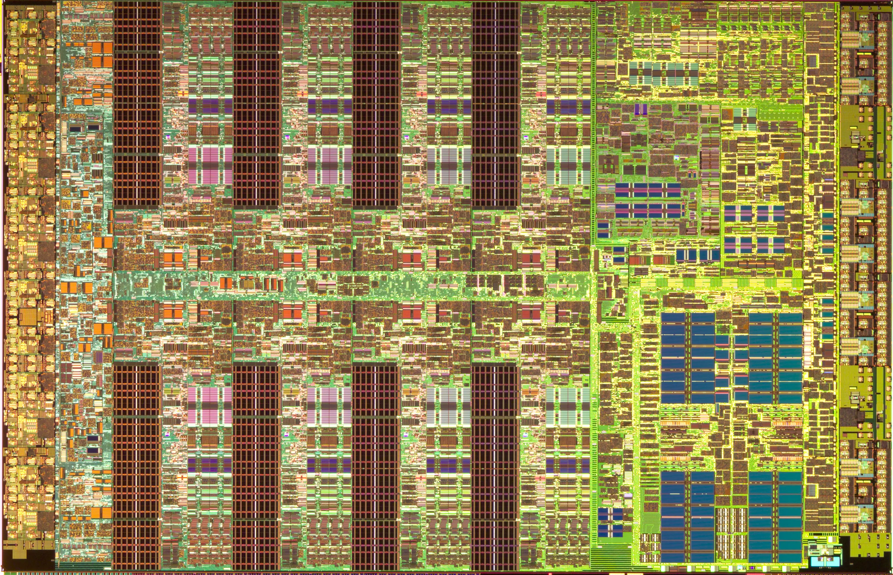
Semitracks provides education, training, certification services, and products for the semiconductor and electronics industries. We specialize in training semiconductor, microsystems, and nanotechnology suppliers and users to understand the dynamic field of electronics technology. View our list of Public Courses and Webinars.
IC Packaging Technology - September 14-15, 2026 (Mon.-Tues.) | Phoenix, AZ - $1,295 $1,195 until Mon. Aug. 24
Advanced CMOS/FinFET Fabrication - September 21-22, 2026 (Mon.-Tues.) | Phoenix, AZ - $1,295 $1,195 until Mon. Aug. 31
Semiconductor Reliability and Product Qualification - February 1-4, 2027 (Mon.-Thurs.) | Cambridge, UK - $2,195 $2,095 until Mon. Jan. 18
Advanced CMOS/FinFET Fabrication - February 16-17, 2027 (Tues.-Wed.) | Dresden, Germany - $1,295 $1,195 until Tues. Jan. 26
Wafer Fab Processing - February 22-25, 2027 (Mon.-Thurs.) | Dresden, Germany - $2,195 $2,095 until Mon. Feb. 1
IC Packaging Technology - March 3-4, 2027 (Wed.-Thurs.) | Munich, Germany - $1,295 $1,195 until Wed. Feb. 10
Failure and Yield Analysis - March 8-11, 2027 (Mon.-Thurs.) | Munich, Germany - $2,195 $2,095 until Mon. Feb. 15
Can't make it to one of our Public Courses? Try our cutting-edge Online Training! Our Online Training helps you learn about the latest developments in many Semiconductor topics including: Failure and Yield Analysis, Reliability, Technology, Process Integration and many others, right from your personal computer. Find out why Semitracks' Online Training is right for you and your company.
Be sure to stop in and browse through our Reference Material. With over 50 pages of material on topics such as Device Recognition, Biased Resistive Contrast Imaging and Acoustic Microscopy, you're sure to find answers to your questions.