System Maintenance occurs every Friday.

Device Recognition

Are you looking for more information regarding this and other subjects? Look no further than Semitracks' Online Training. Semitracks' Online Training contains short courses and other material useful for any Engineer trying to learn new subjects or brush up on old ones.

What is Device Recognition?

Device recognition is the correlation of schematic elements to physical layout structures on the IC. For example, the analyst might need to determine if a particular defect is occurring in a NAND gate or in a D flip-flop. The analyst accomplishes this task by determining what combination of layers implement what devices, building up these individual identifications into a circuit or portion of a circuit.

Device recognition is a useful and many times necessary skill for the failure analyst when he or she is required to relate a physical defect to a particular electrical behavior. Device recognition may also be necessary when layout and schematic information are not available. The skill of correlating a schematic element or elements to physical structures on the IC can mean the difference between properly identifying the failure mechanism and misdiagnosis.

Why Perform Device Recognition?

Device recognition is performed for several different reasons:

  1. Correlate a physical defect with a particular electrical behavior.
  2. The analyst must determine if the physical defect found correlates with the observed electrical behavior in order to determine the failure mechanism. If the local circuitry around the defect is understood, then the failure mechanism can be more quickly verified.
  3. Correlate a layout implementation with a particular electrical behavior.
  4. Sometimes a particular layout can result in incorrect electrical behavior. The ability to understand the local circuitry implementation as well as other factors, such as layout-induced parasitics and leakage paths, determine the outcome of the analysis.
  5. To understand the schematic elements of a local region on the IC.
  6. Many of today's complex ICs are designed from behavioral models, so gate level schematics are never generated. Unfortunately, the failure analyst may need to understand the gate level operation of a circuit in order to diagnose the failure. The ability to recognize circuit elements and construct a portion of the circuitry can greatly aid in understanding the failure.
  7. To reverse engineer an IC.
  8. For some circuits it may be necessary to gain a complete understanding of the electrical behavior of the circuit based on its physical implementation. Reverse engineering may be the only alternative to obtaining the information.

These four reasons constitute the main reasons for performing device recognition. A proficient analyst should be able to produce a schematic from layout data or optical/SEM inspection coupled with some deprocessing.

How is Device Recognition Performed?

Device recognition is typically performed using an optical microscope. Some of today's more advanced technologies require deprocessing and SEM inspection as well. Many regard device recognition as a black art. While today's complex designs can make device recognition difficult, a basic understanding of VLSI design and processing can make this task relatively straightforward. First, a basic understanding of processing is in order.

Bipolar Circuit Design and Layout

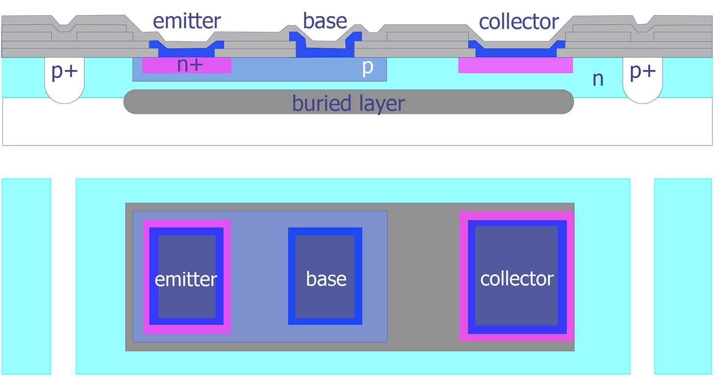
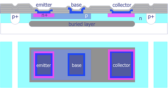
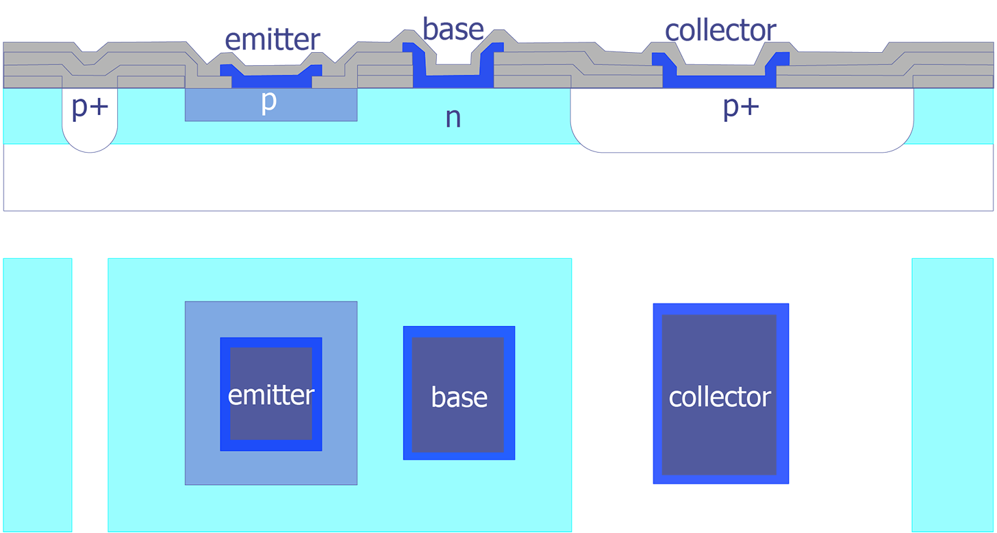
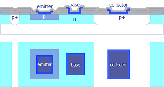
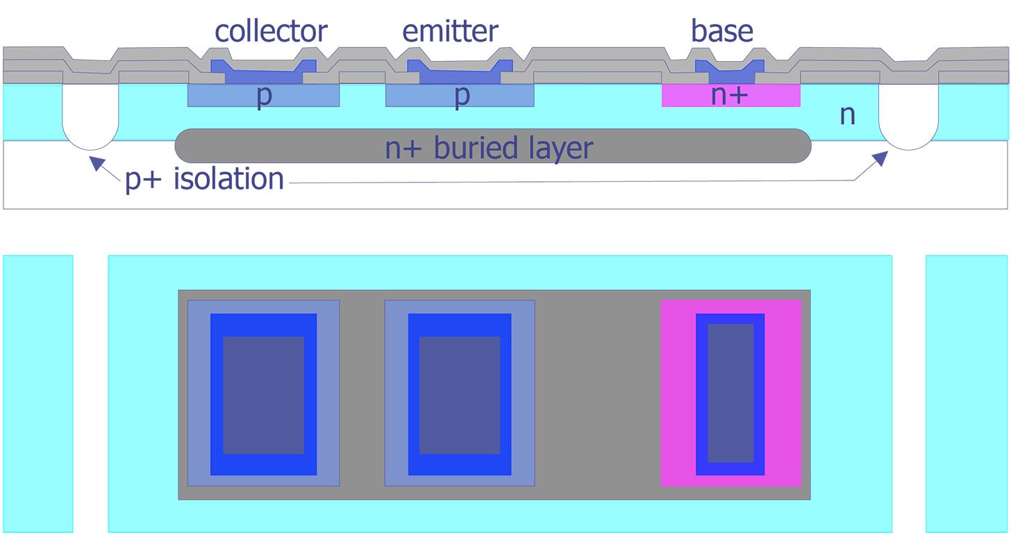
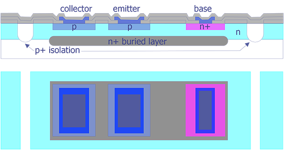
A typical npn bipolar transistor has the following appearance in cross section and top view (see Figure 1). Again, the cross sectional and top view coincide in the horizontal dimension. A substrate pnp bipolar transistor is shown in Figure 2. Although the current gains from this design can be made relatively high, the collector terminal is connected to the substrate, limiting its use in potential designs. Another common pnp transistor design is the lateral pnp transistor (see Figure 3). This transistor has relatively poor transistor gain since the base diffusion is larger. However, it does allow for more flexibility in design.

A basic npn transistor from a bipolar process in cross section and top view (after Maly). A basic npn transistor from a bipolar process in cross section and top view (after Maly).
A basic npn transistor from a bipolar process in cross section and top view (after Maly).
A substrate pnp transistor from a bipolar process in cross section and top view (after Maly). A substrate pnp transistor from a bipolar process in cross section and top view (after Maly).
A substrate pnp transistor from a bipolar process in cross section and top view (after Maly).
A lateral pnp transistor from a bipolar process in cross section and top view (after Maly). A lateral pnp transistor from a bipolar process in cross section and top view (after Maly).
A lateral pnp transistor from a bipolar process in cross section and top view (after Maly).

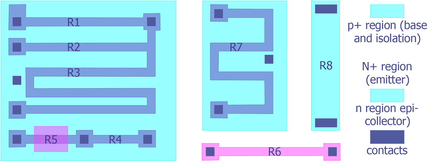
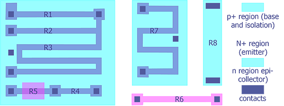
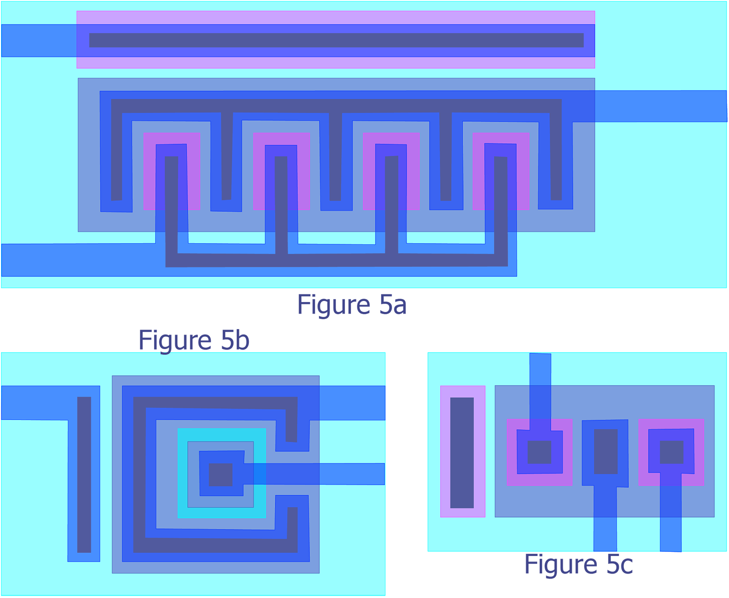
Next, we show a series of layouts demonstrating resistors in the bipolar process. Figure 4 shows an example of this.The following figure shows a series of layouts demostrating several npn and pnp transistors that are different in design than those shown in Figs. 1 through 3 (see Figure 5). Finally, a bipolar circuit exhibiting an R-S flip flop is shown in Figure 6. The schematic is shown in Figure 7. At this point, it is also worthwhile to show an oxide isolated bipolar process (see Figure 8). This process is more commonly used for today's bipolar circuitry because it eliminates the need for larger spacing between devices by using an oxide spacer between devices. The parasitic capacitances are also reduced, allowing the circuitry to switch faster.

Several examples of resistors in a bipolar technology. R1, R2, R3 are base resistors, R5 is a base pinch resistor (emitter region creates a pinched channel, raiseing the resistance of R5 so less area is required), R6 is an emitter resistor (low ohmage resistor), R7 is also a base resistor - used for a different application than R1-R3 (since it is isolated in a separate tub from R1-R5). The epi-collector contacts associated with R1-R5 and R7 provide a fixed voltage for the region. R8 is an epitaxiatial resitor for high ohmage requirements (after Maly). Several examples of resistors in a bipolar technology. R1, R2, R3 are base resistors, R5 is a base pinch resistor (emitter region creates a pinched channel, raiseing the resistance of R5 so less area is required), R6 is an emitter resistor (low ohmage resistor), R7 is also a base resistor - used for a different application than R1-R3 (since it is isolated in a separate tub from R1-R5). The epi-collector contacts associated with R1-R5 and R7 provide a fixed voltage for the region. R8 is an epitaxiatial resitor for high ohmage requirements (after Maly).
Several examples of resistors in a bipolar technology. R1, R2, R3 are base resistors, R5 is a base pinch resistor (emitter region creates a pinched channel, raiseing the resistance of R5 so less area is required), R6 is an emitter resistor (low ohmage resistor), R7 is also a base resistor - used for a different application than R1-R3 (since it is isolated in a separate tub from R1-R5). The epi-collector contacts associated with R1-R5 and R7 provide a fixed voltage for the region. R8 is an epitaxiatial resitor for high ohmage requirements (after Maly).
Figure 5a npn transistor with multiple emitter wells. The multiple emitter wells allow this device to handle higher current, making it useful to drive signals off the die (commonly used for creating I/O structures). Figure 5b Lateral pnp transistor. The ring structure provides better minority carrier injection, which results in better gain and hence better device performance. Figure 5c An npn transistor with multiple emitters. Multiple emitters create an easy way to create some logic functions like multiple input gates (e.g. 2 NAND, 2NOR, etc.). Figure 5a npn transistor with multiple emitter wells. The multiple emitter wells allow this device to handle higher current, making it useful to drive signals off the die (commonly used for creating I/O structures). Figure 5b Lateral pnp transistor. The ring structure provides better minority carrier injection, which results in better gain and hence better device performance. Figure 5c An npn transistor with multiple emitters. Multiple emitters create an easy way to create some logic functions like multiple input gates (e.g. 2 NAND, 2NOR, etc.).
Figure 5a npn transistor with multiple emitter wells. The multiple emitter wells allow this device to handle higher current, making it useful to drive signals off the die (commonly used for creating I/O structures). Figure 5b Lateral pnp transistor. The ring structure provides better minority carrier injection, which results in better gain and hence better device performance. Figure 5c An npn transistor with multiple emitters. Multiple emitters create an easy way to create some logic functions like multiple input gates (e.g. 2 NAND, 2NOR, etc.).
Layout of the composite drawing of an RS flip-flop. Circuit element labels correspond to the schematic shown in Figure 7 (after Glaser and Subak-Sharpe). Layout of the composite drawing of an RS flip-flop. Circuit element labels correspond to the schematic shown in Figure 7 (after Glaser and Subak-Sharpe).
Layout of the composite drawing of an RS flip-flop. Circuit element labels correspond to the schematic shown in Figure 7 (after Glaser and Subak-Sharpe).
Circuit schematic for Figure 6 (after Glaser and Subak-Sharpe). Circuit schematic for Figure 6 (after Glaser and Subak-Sharpe).
Circuit schematic for Figure 6 (after Glaser and Subak-Sharpe).
An oxide isolated bipolar technology process showing the layout of the cell and cross-section of the process (after Maly). An oxide isolated bipolar technology process showing the layout of the cell and cross-section of the process (after Maly).
An oxide isolated bipolar technology process showing the layout of the cell and cross-section of the process (after Maly).

NMOS Circuit Design and Layout

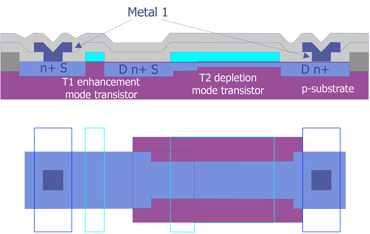
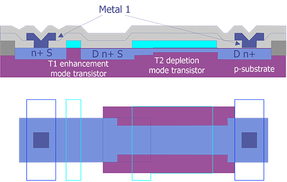
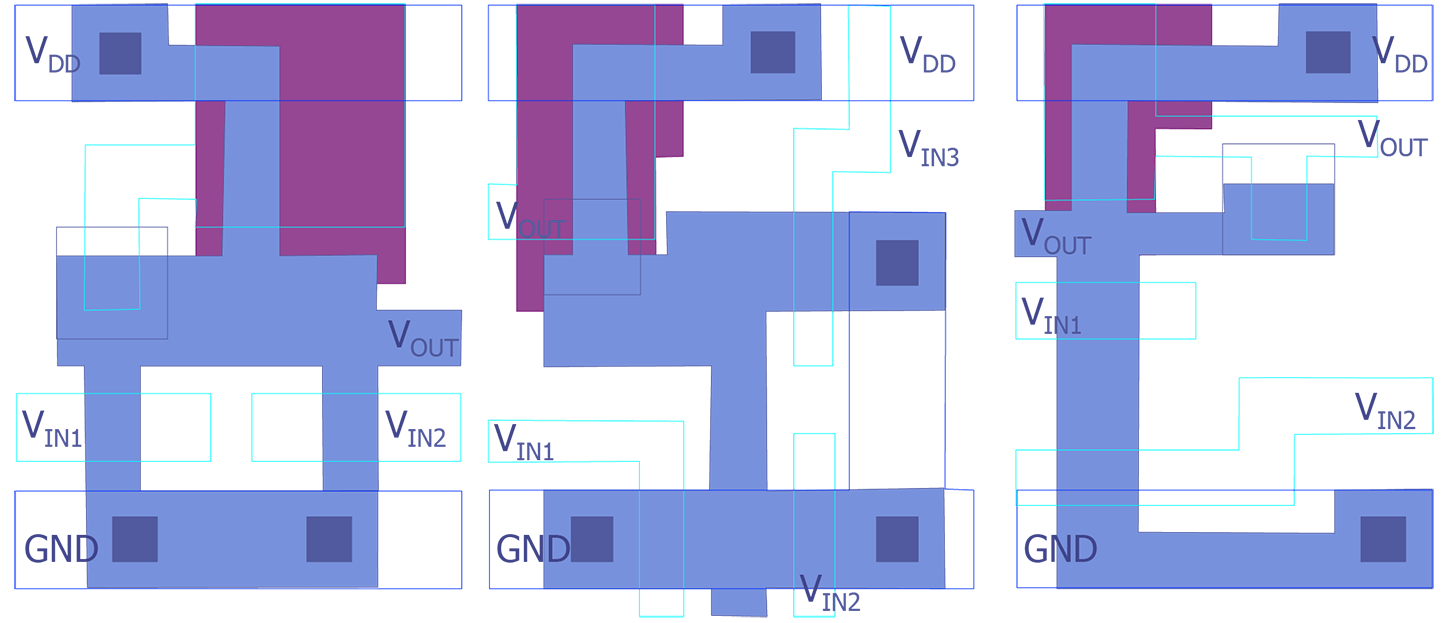
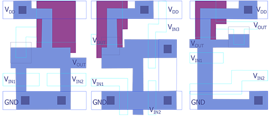
A typical NMOS process has the following appearance in cross section and top view (see Figure 9). The cross sectional and top view directly coincide in horizontal dimension so that you can see the relationship of various layers to structures in the top view. NMOS technology uses a depletion mode transistor as the pull-up transistor in an inverter structure. Next, a series of NMOS cells are shown, including a two input NOR gate, a three input NOR gate, a NAND gate (see Figure 10), and an RS flip-flop composed of cross-coupled NOR gates (see Figures 11a-11g).

A typical NMOS process in cross section and top view (after Maly). A typical NMOS process in cross section and top view (after Maly).
A typical NMOS process in cross section and top view (after Maly).
Figure 10a (left) An NMOS NOR gate composite layout (after Maly). Figure 10b (center) A three input NMOS NOR gate composite layout (after Maly). Figure 10c (right) An NMOS NAND gate composite layout (after Maly). Figure 10a (left) An NMOS NOR gate composite layout (after Maly). Figure 10b (center) A three input NMOS NOR gate composite layout (after Maly). Figure 10c (right) An NMOS NAND gate composite layout (after Maly).
Figure 10a (left) An NMOS NOR gate composite layout (after Maly). Figure 10b (center) A three input NMOS NOR gate composite layout (after Maly). Figure 10c (right) An NMOS NAND gate composite layout (after Maly).
Composite drawing of the layout for a cross-coupled NOR gate version of the RS flip-flop (after Maly). Composite drawing of the layout for a cross-coupled NOR gate version of the RS flip-flop (after Maly).
Composite drawing of the layout for a cross-coupled NOR gate version of the RS flip-flop (after Maly).

CMOS Circuit Design and Layout

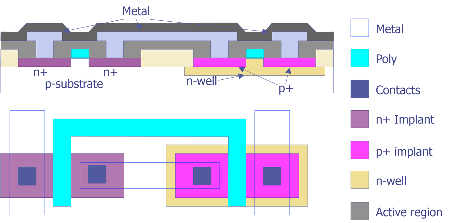
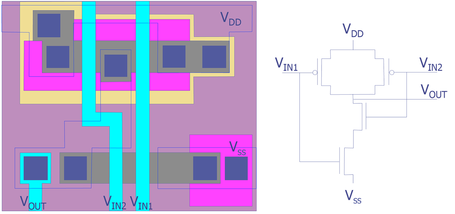
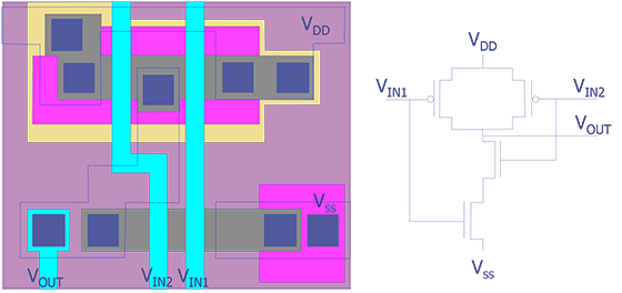
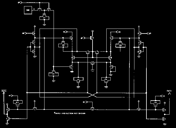
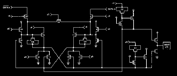
A typical n-well CMOS process has the following appearance in cross section and top view (see Figure 12). The cross-sectional and top view directly coincide in horizontal dimension so that you can see the relationship of various layers to structures in the top view. Next, we show a layout and schematic for a 2 input NAND gate (see Figure 13).

A typical-well CMOS process in cross section and top view (after Pradhan and Singh). A typical-well CMOS process in cross section and top view (after Pradhan and Singh).
A typical-well CMOS process in cross section and top view (after Pradhan and Singh).
Composite layout and schematic of a 2 input CMOS NAND gate (after Maly). Composite layout and schematic of a 2 input CMOS NAND gate (after Maly).
Composite layout and schematic of a 2 input CMOS NAND gate (after Maly).

Memory Structures

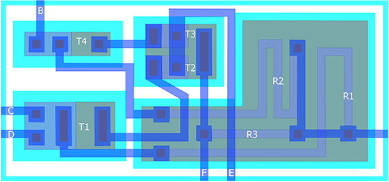
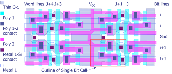
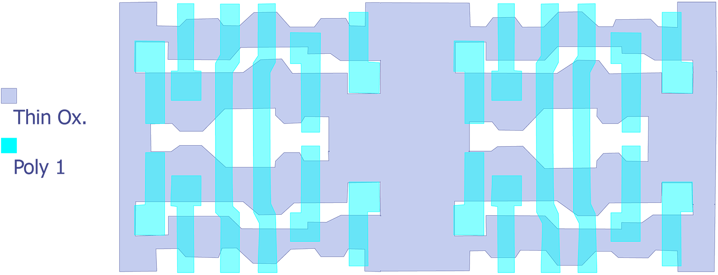
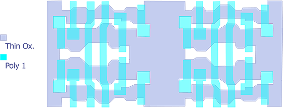
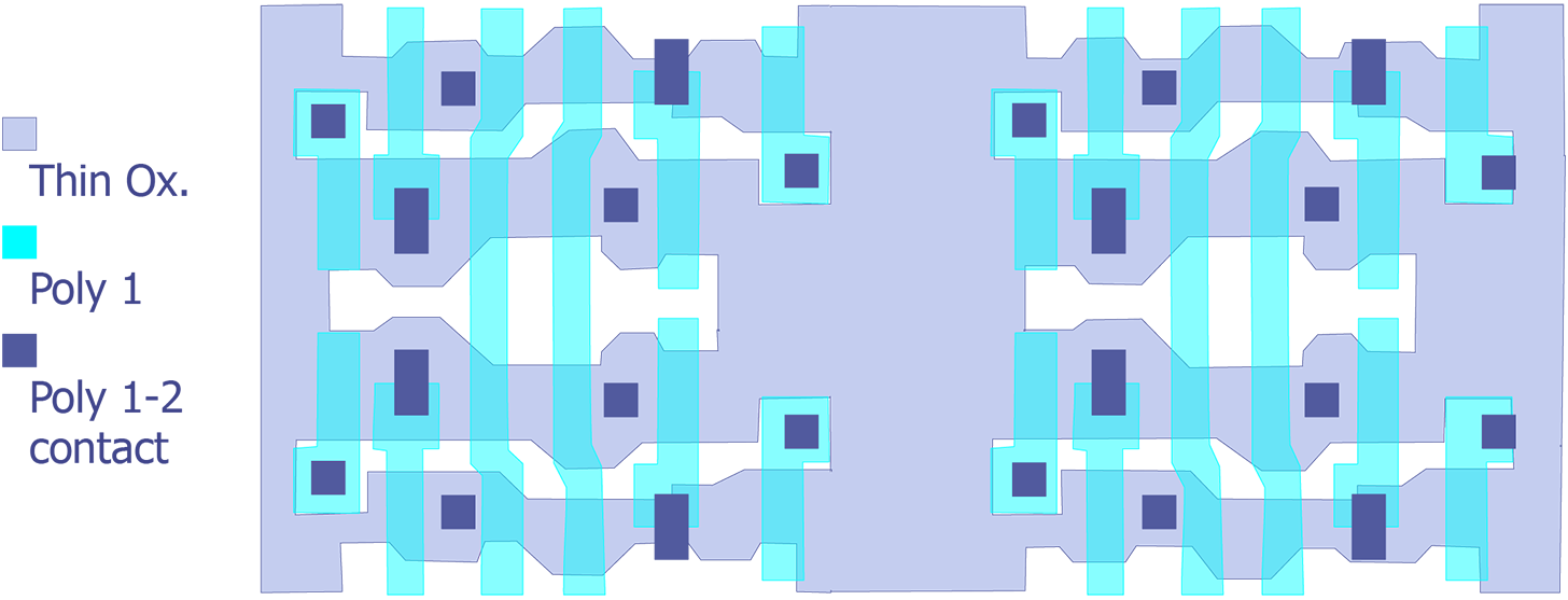
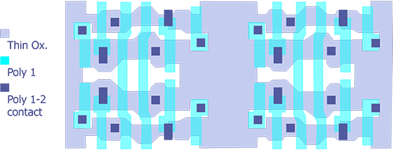
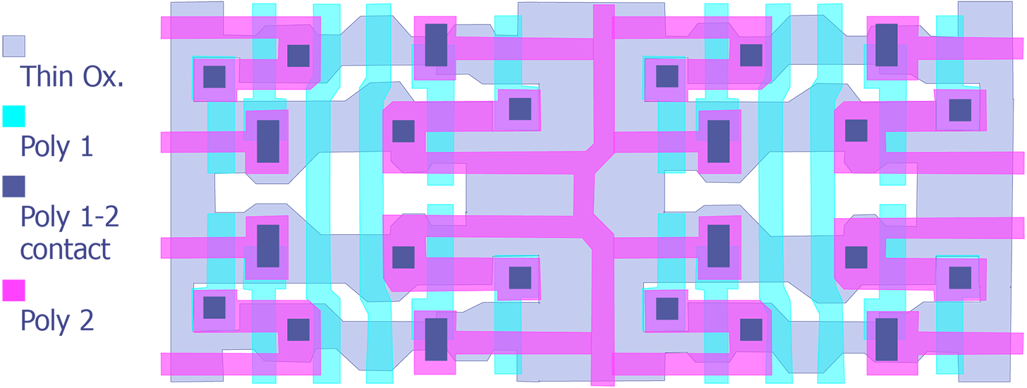
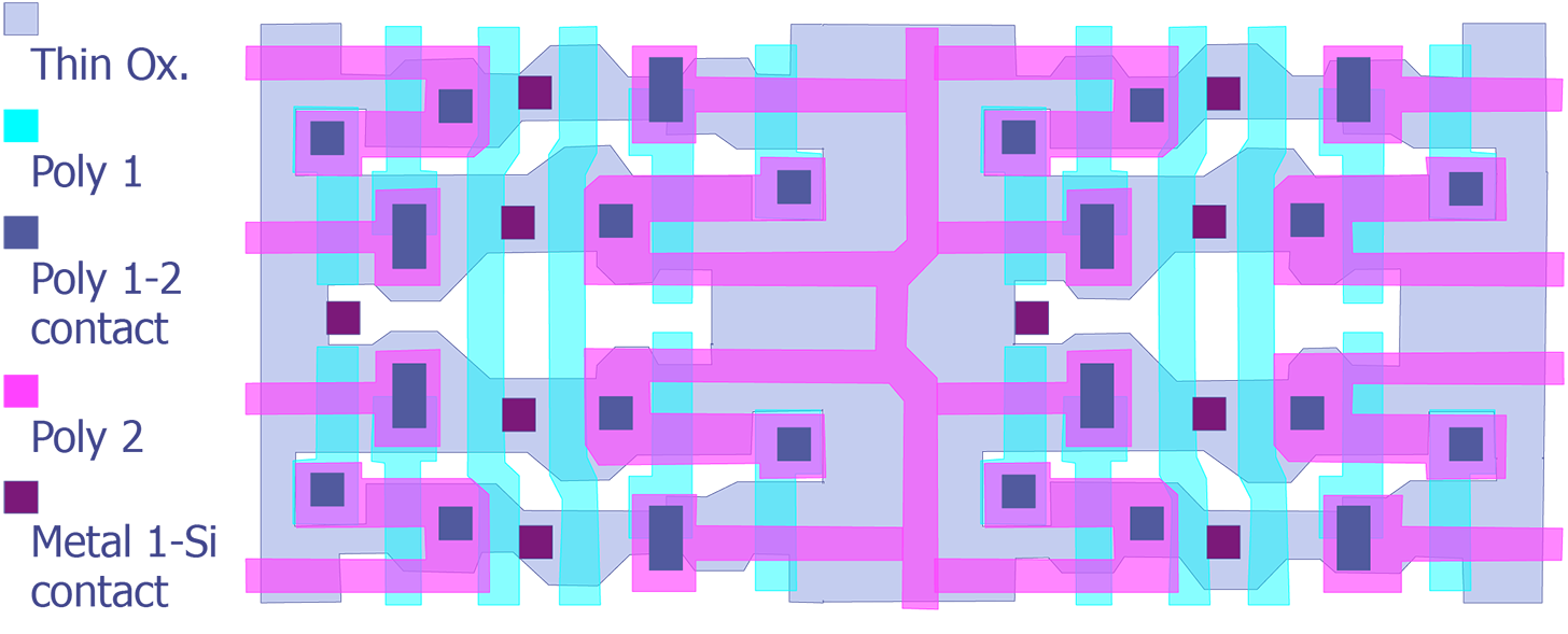
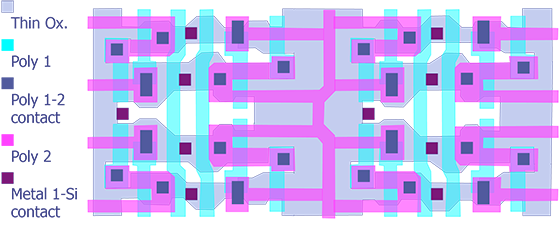
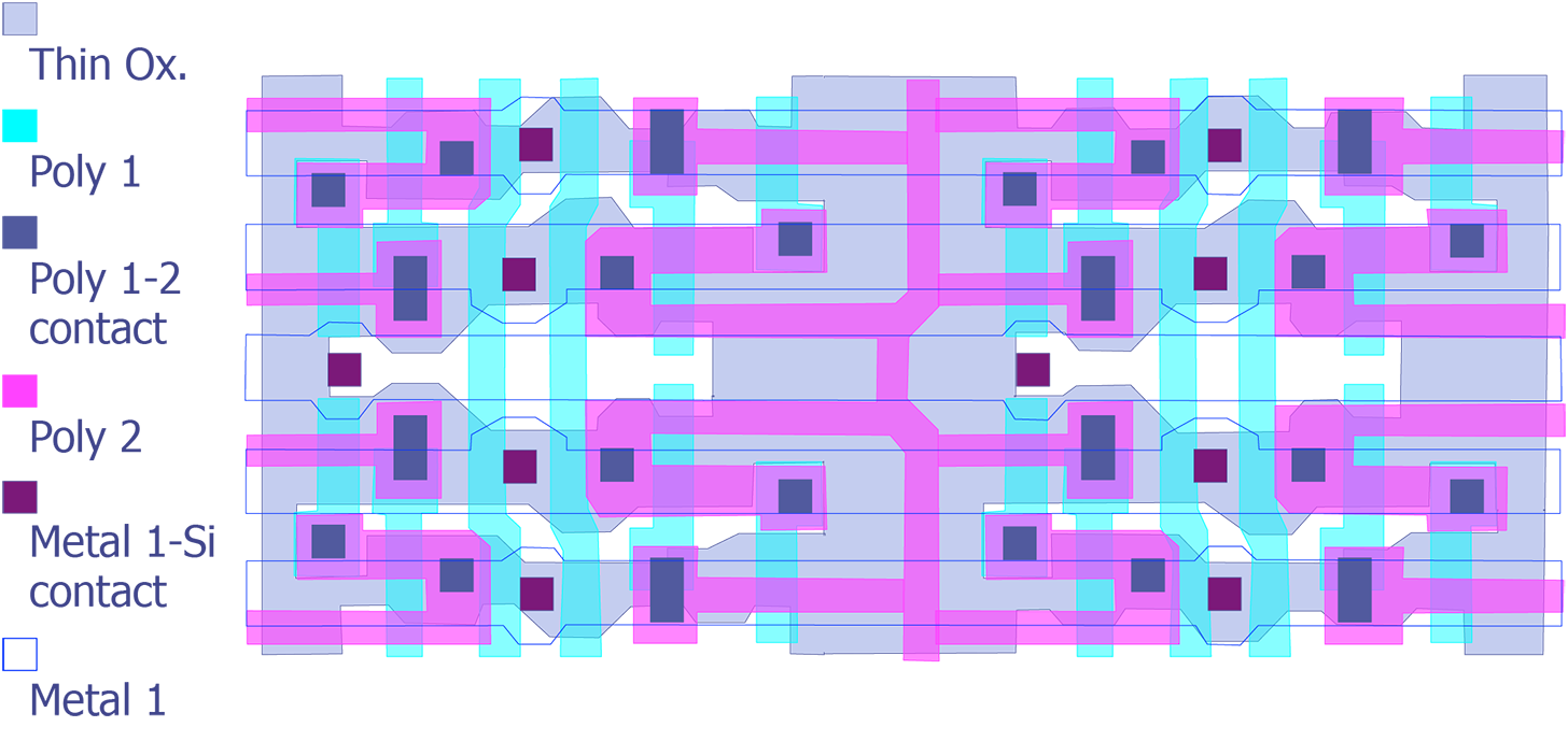
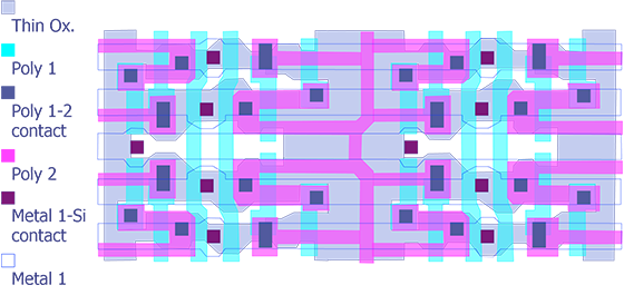
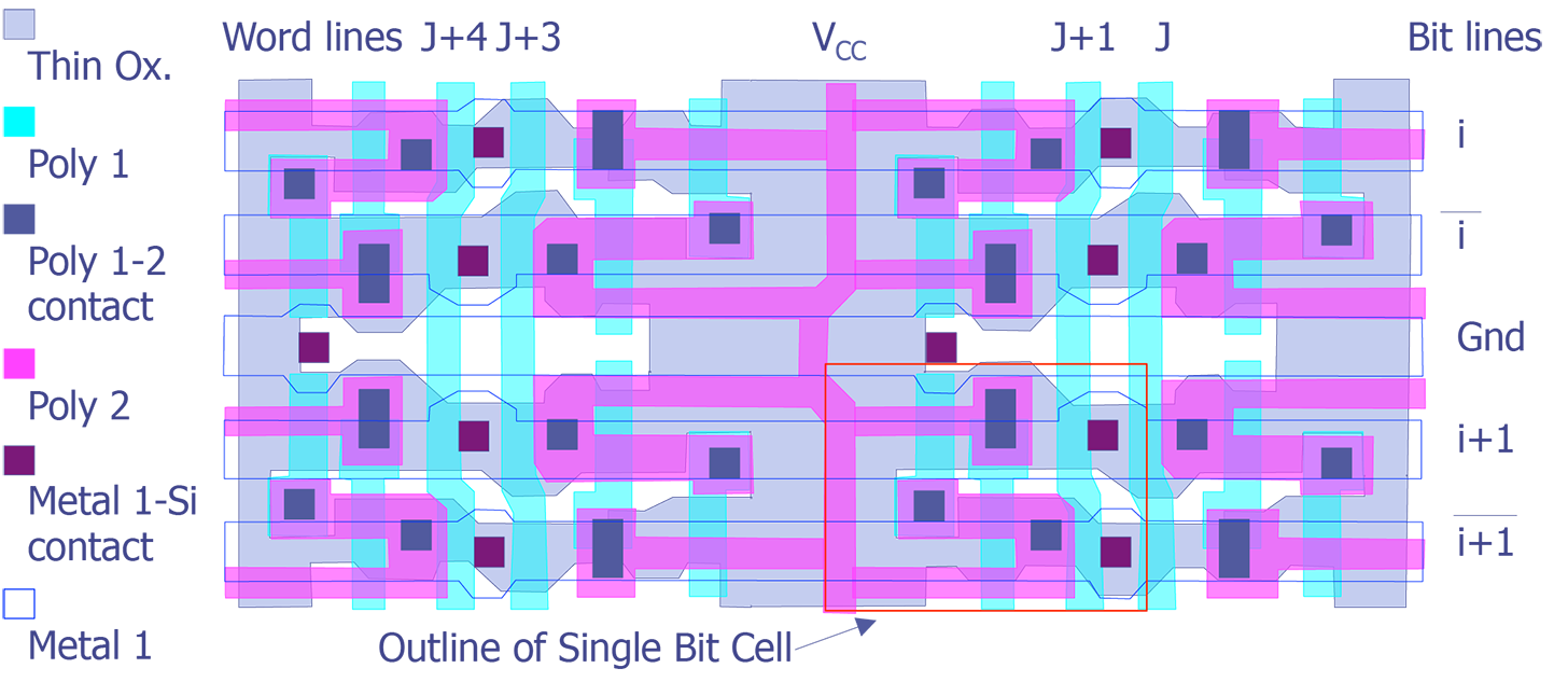
Now that we have examined the basic structures for bipolar, NMOS and CMOS technologies, let's examine memory structures. We will first discuss the CMOS Static Random Access Memory (SRAM). There are two major classes of design in CMOS SRAMs: the four transistor design and the six transistor design. Figure 14 shows both designs in electrical schematic format. Figure 15 shows the layout of the four transistor design. Figures 11a-11g show a step-by-step model of the patterning for this memory.

Schematic of the four and six transistor SRAM memory designs. Schematic of the four and six transistor SRAM memory designs.
Schematic of the four and six transistor SRAM memory designs.
Complete layout of an 8-bit segment of the four transistor SRAM memory design with highlighted word, bit, ground and V sub CC lines (after Maly). Complete layout of an 8-bit segment of the four transistor SRAM memory design with highlighted word, bit, ground and V sub CC lines (after Maly).
Complete layout of an 8-bit segment of the four transistor SRAM memory design with highlighted word, bit, ground and VCC lines (after Maly).

When is Device Recognition Performed?

Device recognition is typically done once a suspect physical defect or layout abnormality is found. It is typically performed during optical examination with a high power microscope; however, the scanning electron microscope, scanning laser microscope and focused ion beam tools can also augment device recognition by providing higher quality or different contrast images. It may be necessary to perform the device recognition in two phases, one with all the metal layers intact and two with the IC stripped down to metal 1 or poly. If multiple ICs are available, this activity can proceed in parallel with other analysis activities.

If a significant amount of reverse engineering will be necessary to understand circuit operation, consult with the requestor and your management. Layout reverse engineering is very time consuming and should not be performed unless absolutely necessary.


References on Device Recognition

  1. W. Maly, An Atlas of IC Technology, Benjamin/Cummings, 1990.
  2. D. Pradhan and A. Singh, VLSI Design Short Course Notes, 1996
  3. N. Weste and K. Eshraghian, Principles of CMOS VLSI Design, Addison Wesley, Second Ed., 1993
  4. H. K. Dicken, Physics of Semiconductor Failures, Third Edition, DM Data, pp. 129-161, 1989.
  5. E. Doyle and B. Morris, eds., Failure Analysis Techniques - A Procedural Guide, IITRI, pp. I-3-50, 1980.
Photograph of an NMOS 64k SRAM showing its various blocks. This photograph serves as a basis for Figs. 2-10. (photo courtesy ICE Corp). Photograph of an NMOS 64k SRAM showing its various blocks. This photograph serves as a basis for Figs. 2-10. (photo courtesy ICE Corp).
Figure 1. Photograph of an NMOS 64k SRAM showing its various blocks. This photograph serves as a basis for Figs. 2-10. (photo courtesy ICE Corp).
Photograph of an address buffer on the NMOS 64k SRAM showing power, ground and signal lines. (photo courtesy ICE Corp). Photograph of an address buffer on the NMOS 64k SRAM showing power, ground and signal lines. (photo courtesy ICE Corp).
Figure 2. Photograph of an address buffer on the NMOS 64k SRAM showing power, ground and signal lines. (photo courtesy ICE Corp).
Photograph of the address buffer after the IC was stripped to polysilicon. Locations of individual transistors are shown. (photo courtesy ICE Corp). Photograph of the address buffer after the IC was stripped to polysilicon. Locations of individual transistors are shown. (photo courtesy ICE Corp).
Figure 3. Photograph of the address buffer after the IC was stripped to polysilicon. Locations of individual transistors are shown. (photo courtesy ICE Corp).
Circuit schematic of the address buffer. Numbers on the circuit elements correlate to the numbers in Figure 3. (photo courtesy ICE Corp). Circuit schematic of the address buffer. Numbers on the circuit elements correlate to the numbers in Figure 3. (photo courtesy ICE Corp).
Figure 4. Circuit schematic of the address buffer. Numbers on the circuit elements correlate to the numbers in Figure 3. (photo courtesy ICE Corp).
Photograph of data-in circuit on the NMOS 64k SRAM showing power, ground and signal lines. (photo courtesy ICE Corp). Photograph of data-in circuit on the NMOS 64k SRAM showing power, ground and signal lines. (photo courtesy ICE Corp).
Figure 5. Photograph of data-in circuit on the NMOS 64k SRAM showing power, ground and signal lines. (photo courtesy ICE Corp).
Photograph of the data-in circuit after the IC was stripped to polysilicon. Locations of the transistors are shown. (photo courtesy ICE Corp). Photograph of the data-in circuit after the IC was stripped to polysilicon. Locations of the transistors are shown. (photo courtesy ICE Corp).
Figure 6. Photograph of the data-in circuit after the IC was stripped to polysilicon. Locations of the transistors are shown. (photo courtesy ICE Corp).
Circuit schematic of the data-in circuit. Numbers on the circuit elements correlate to the numbers in Figure 6. (photo courtesy ICE Corp). Circuit schematic of the data-in circuit. Numbers on the circuit elements correlate to the numbers in Figure 6. (photo courtesy ICE Corp).
Figure 7. Circuit schematic of the data-in circuit. Numbers on the circuit elements correlate to the numbers in Figure 6. (photo courtesy ICE Corp).
Photograph of the data-out circuit on the NMOS 64k SRAM showing power, ground and signal lines. (photo courtesy ICE Corp). Photograph of the data-out circuit on the NMOS 64k SRAM showing power, ground and signal lines. (photo courtesy ICE Corp).
Figure 8. Photograph of the data-out circuit on the NMOS 64k SRAM showing power, ground and signal lines. (photo courtesy ICE Corp).
Photograph of the data-out circuit after the IC was stripped to polysilicon. Locations of individual transistors are shown. (photo courtesy ICE Corp). Photograph of the data-out circuit after the IC was stripped to polysilicon. Locations of individual transistors are shown. (photo courtesy ICE Corp).
Figure 9. Photograph of the data-out circuit after the IC was stripped to polysilicon. Locations of individual transistors are shown. (photo courtesy ICE Corp).
Circuit schematic of the data-out circuit. Numbers on the circuit elements correlate to the numbers in Figure 9. (photo courtesy ICE Corp). Circuit schematic of the data-out circuit. Numbers on the circuit elements correlate to the numbers in Figure 9. (photo courtesy ICE Corp).
Figure 10. Circuit schematic of the data-out circuit. Numbers on the circuit elements correlate to the numbers in Figure 9. (photo courtesy ICE Corp).

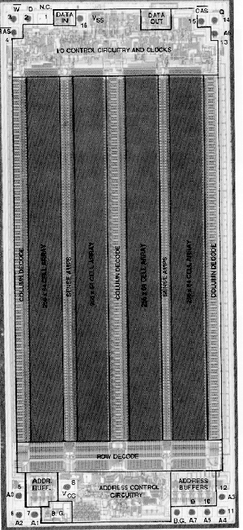
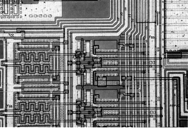
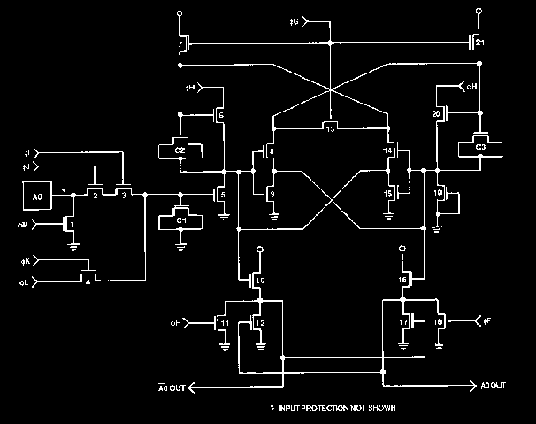
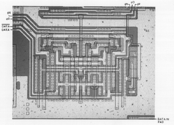
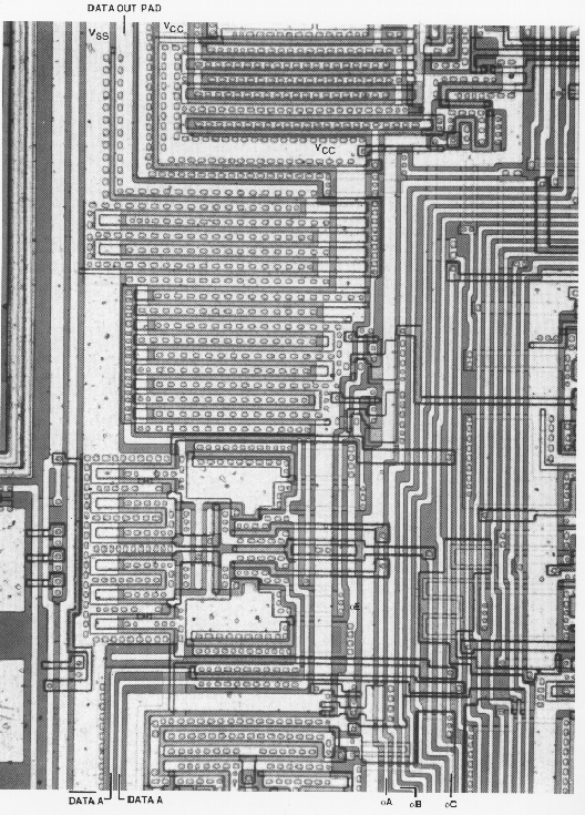
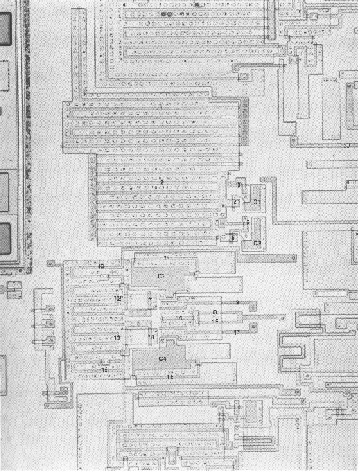
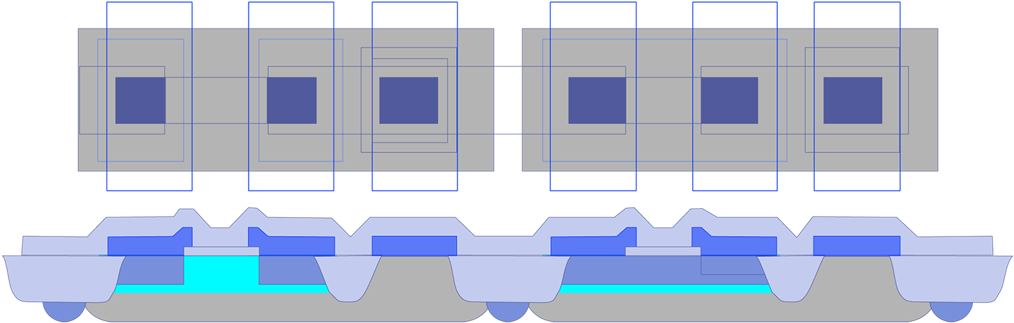
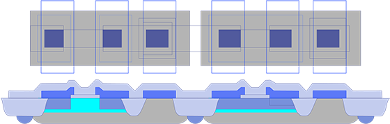
Graphic sequence describing the major mask levels for a 4 transistor cell 64k Static Random Access Memory (SRAM) manufactured by Fairchild Semiconductor Research Center.

Figure 11-1. Thin oxide mask for the 64k SRAM (after Maly). Figure 11-1. Thin oxide mask for the 64k SRAM (after Maly).
Figure 11-1. Thin oxide mask for the 64k SRAM (after Maly).
Figure 11-2. Poly mask (shown in cyan) for the 64k SRAM (after Maly). Figure 11-2. Poly mask (shown in cyan) for the 64k SRAM (after Maly).
Figure 11-2. Poly mask (shown in cyan) for the 64k SRAM (after Maly).
Figure 11-3. Contact windows to the active regions (shown in purple) for the 64k SRAM. The rectangular contacts contact the second level of poly as well (after Maly). Figure 11-3. Contact windows to the active regions (shown in purple) for the 64k SRAM. The rectangular contacts contact the second level of poly as well (after Maly).
Figure 11-3. Contact windows to the active regions (shown in purple) for the 64k SRAM. The rectangular contacts contact the second level of poly as well (after Maly).
Figure 11-4. Mask for second level of polysilicon (shown in magenta) for the 64k SRAM (after Maly). Figure 11-4. Mask for second level of polysilicon (shown in magenta) for the 64k SRAM (after Maly).
Figure 11-4. Mask for second level of polysilicon (shown in magenta) for the 64k SRAM (after Maly).
Figure 11-5. Mask for the metal to silicon contacts (shown in maroon) for the 64k SRAM (after Maly). Figure 11-5. Mask for the metal to silicon contacts (shown in maroon) for the 64k SRAM (after Maly).
Figure 11-5. Mask for the metal to silicon contacts (shown in maroon) for the 64k SRAM (after Maly).
Figure 11-6. Mask for the metal lines (shown in blue outline) for the 64k SRAM (after Maly). Figure 11-6. Mask for the metal lines (shown in blue outline) for the 64k SRAM (after Maly).
Figure 11-6. Mask for the metal lines (shown in blue outline) for the 64k SRAM (after Maly).
Figure 11-7. Complete layout of an 8-bit segment of the four transistor 64k SRAM memory design with highlighted word, bit, ground and V sub CC lines (after Maly). Figure 11-7. Complete layout of an 8-bit segment of the four transistor 64k SRAM memory design with highlighted word, bit, ground and V sub CC lines (after Maly).
Figure 11-7. Complete layout of an 8-bit segment of the four transistor 64k SRAM memory design with highlighted word, bit, ground and VCC lines (after Maly).