System Maintenance occurs every Friday.
System Maintenance occurs every Friday.
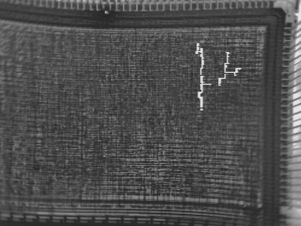
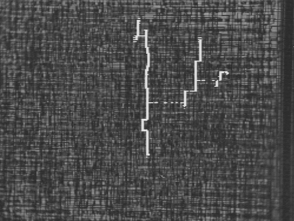
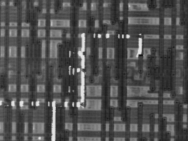
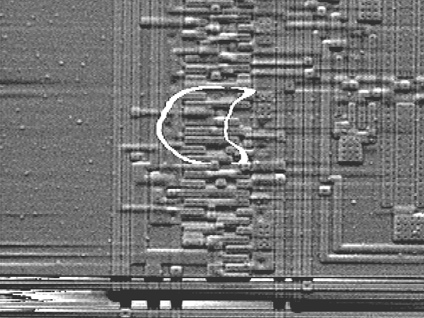
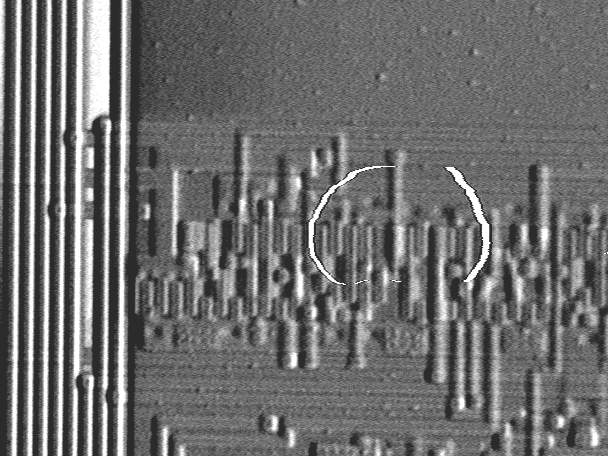
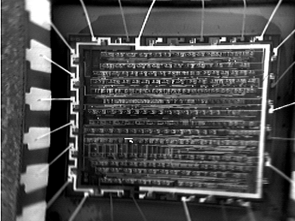
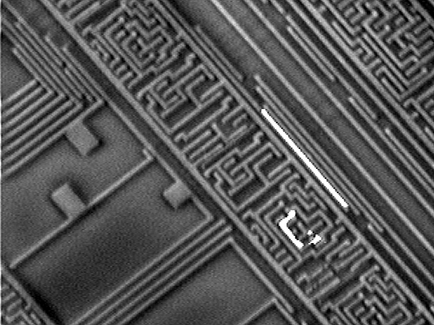
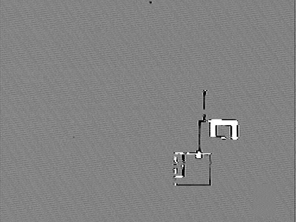
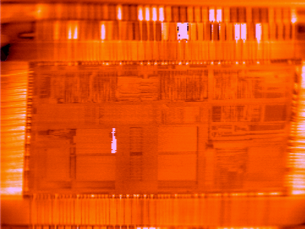
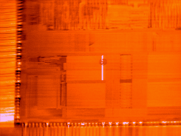
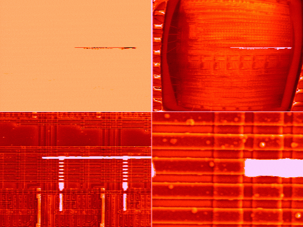
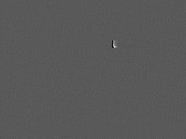
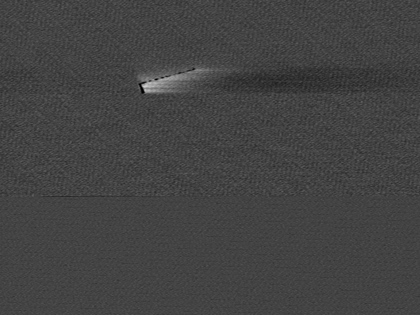
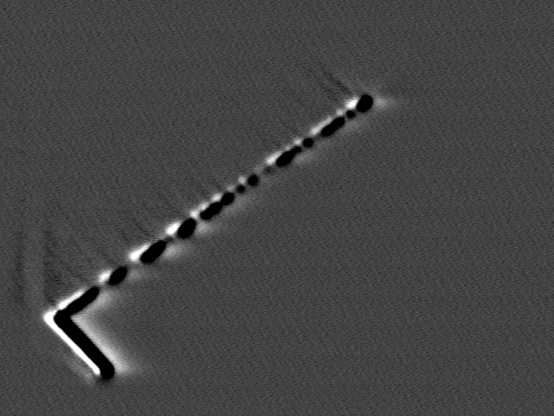
Charge-Induced Voltage Alteration (CIVA, pronounced "kiva") imaging of biased ICs is a new scanning electron microscopy imaging technique developed to localize open conductors. CIVA may be applied to both passivated and depassivated multi-level interconnect ICs. Contrast variations in images produced using the CIVA technique are generated only from the electrically open portion of the conductor. This feature facilitates the examination of an entire IC for opens from a single, unprocessed image. Examples of CIVA imaging at various magnifications of a stress-induced metal void are shown below.
Electrically open conductors on integrated circuits (ICs) may be defined as conducting pathways whose ability to transfer electrical signals from one part of the IC to another has been compromised by one or more failure mechanisms. A great deal of research has examined various mechanisms, including stress voiding, electromigration, Si migration in contacts, and design and processing defects, that produce open conductors. The large effort to understand these mechanisms indicates the serious and ubiquitous nature of this potential problem.
The detection and localization of open conductors in ICs has become more difficult as line widths are reduced and IC complexity increases. A number of scanning electron microscopy techniques, such as static and dynamic voltage contrast, resistive contrast imaging, and biased resistive contrast imaging, have been developed to localize open conductors. Unfortunately, each of these methods has two limitations in detecting open conductors. (1) A great deal of superfluous information in the images complicates the extraction of open circuit information. (2) Opens with a significant amount of quantum mechanical electron tunneling, such as opens resulting from electromigration and stress voiding, are very difficult to detect.
Charge-Induced Voltage Alteration (CIVA) imaging of biased ICs is designed to overcome the above limitations. For passivated ICs, CIVA requires a lower primary electron beam energies than static voltage contrast imaging requires. Using lower primary electron beam energies greatly reduces irradiation damage to gate oxides by primary electrons and lowers the bremsstrahlung x-ray dose. Experimental work indicates that CIVA imaging may be applied without undue degradation effects to gate oxides.
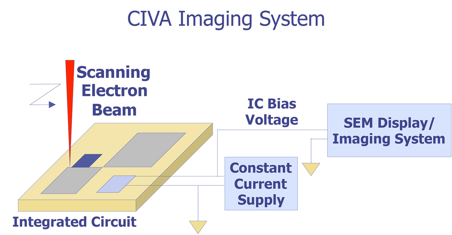
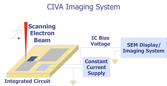
CIVA is analogous to electron beam induced current (EBIC) imaging in that the biased IC itself is the detector and amplifier. The signal monitored to produce a CIVA image is the power supply voltage of a constant current source used to bias the IC as the electron beam is scanned across the device surface (see Figure 1).
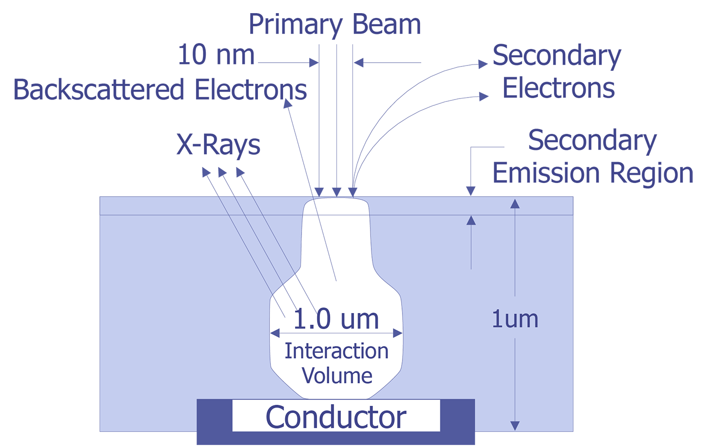
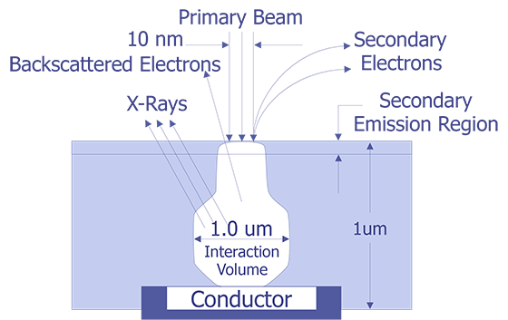
To produce the CIVA signal, the primary electron beam must penetrate to the conductors of the IC, as shown in Figure 2. If a conductor is electrically open, the charge injected into the conductor by the primary electron beam can reduce the voltage of the conductor and greatly affect the voltage demands of the IC supplied by a constant current source. As opposed to biased resistive contrast imaging, CIVA is not currently limited by any deleterious factors.
The response of a CMOS inverter pair to various gate biases was examined (see Figure 3) to illustrate how changes in conductor voltages generate the CIVA signal. The inverter pair was fabricated using a 3 micron, polysilicon gate, n-well process with VTN = 0.76 V and VTP = -0.77 V. By using an inverter pair as our test structure the loading on the drain of the first inverter would be representative of that found on an IC. The inverter was supplied with a constant current source of 20 nanoamps and a compliance voltage of 5 volts.
The results of voltage sweeps from 5 volts to -1 volts on separate n- and p-transistor gates of the first inverter pair are shown in Figure 4 and Figure 5. In Figure 4, the gate of the n-channel transistor is connected to the constant current source (IDD = 20 nanoamps) and the gate of the p-channel transistor is swept from 5 to -1 volts. With approximately 4.3 volts on the p-channel gate, the power supply voltage begins to drop on the constant current source supplying the inverter pair. The decrease in the supply voltage at constant current is linear down to the threshold voltage (~0.7 volts). This supply voltage drop is linear because the p-channel transistor is operating in the ohmic region until the gate voltage reaches 0 volts. The supply voltage does not drop below the transistor threshold voltage because no current flows from VDD to VSS occurs with supply voltages lower than threshold.
In Figure 5, the gate of the p-channel transistor is connected to ground and the n-channel transistor gate is swept from 5 to -1 volts. The power supply voltage remains at 0.7 volts until the n-channel gate bias reaches approximately 0.7 volts. The power supply bias increases abruptly with n-channel gate voltages below 0.7 volts. The power supply voltage remains at 0.7 volts for gate voltages above 0.7 volts because the n-channel transistor is in saturation until the gate voltage reaches threshold. Below 0.7 volts, the n-channel transistor "turns off" abruptly, achieving the 5-volt compliance voltage.
Figure 6 displays the results of sweeping the voltage with both input gates tied together. As may be expected, the resulting curve is a superposition of Figure 4 and Figure 5. The output of the first inverter at V1 in Figure 3 is also shown in Figure 6.


In Figures 4 and 6, the power supply voltage drops significantly as the gate bias is reduced below 4.3 volts. An even more dramatic increase in power supply voltage occurs in Figures 5 and 6 as the gate bias is reduced below 0.7 volts. CIVA imaging takes advantage of these changes in a constant current power supply voltage with changes in gate bias. The CIVA images display the conductors, which are susceptible to voltage change by small amounts of injected charge, i.e. open conductors.
The bias configuration of the IC for CIVA examination may be any non-contention state. The static burn-in configuration used for IC burn-in and life testing is an example of an appropriate bias configuration.
While surface emission products like secondary electrons are not used to produce the CIVA image, they are a factor in image formation on passivated ICs. In order to penetrate nearly through typical passivation layers, the primary electron beam energy must be increased to 5 keV or above. At these beam energies, more electrons are injected into the passivation layer than the number that escape through backscattered and secondary electron emission. On the surface, a negative potential builds up that can effectively put all of the transistor gates into a low state, eliminating all IC functionality. As the primary electron beam energy is increased until the interaction volume reaches buried conductors, a new current path is produced. Charge can leave the passivation layer through the biased IC conductors and substrate. This additional current path reduces the negative charge of the passivation and permits normal operation of the IC. Voltage contrast observation may still be obscured by surface charging from areas with passivation thicker than that over the conductors, but the CIVA signal is not affected by this charging. The small added amount of charge from the electron beam has little effect on the IC operating characteristics of non-failing ICs, changing the power supply current by nanoamps. This is because the voltage drive of the transistors on CMOS devices can easily compensate for nanoamps, and in some cases microamps, of additional current.
The proper primary electron beam energy for CIVA imaging on passivated CMOS ICs is selected by first biasing the IC with a constant voltage source and the electron beam off. The IC current is then monitored as the primary electron beam energy is increased. The entire IC die is scanned at a rapid rate (TV scan rate) as the primary electron beam energy is increased. Initially, the IC current will increase as the surface charges negatively, then decrease when the primary electron interaction volume intersects the buried conductors. Because most scanning electron microscopes change electron beam energy in 1 keV steps above 5 keV, the IC current will fall abruptly. Primary electron beam energies above this should not be used in order to reduce irradiation effects, as discussed below.
For depassivated ICs, the conductors are directly on the surface, and very low primary electron beam energies are required to inject charge into these conductors. A primary electron beam energy of 300 eV was used for our CIVA imaging of depassivated ICs.
Once the proper primary electron beam energy is selected, the IC current (IDDQ) under constant voltage conditions is recorded. For static CMOS ICs, IDDQ is normally several microamps or less. A current value slightly (5%) less than this operates the IC with the constant current source. The resulting voltage powering the IC is approximately that used under constant voltage source conditions. A compliance voltage limit prevents any accidental damage to the IC from the constant current source. For all CIVA results reported here, a compliance voltage of 5 volts was used.
Open conductors can be grouped into two categories for CIVA imaging: (1) conductors that are open "complete" and communicate no significant electrical signal across the site of the open and (2) conductors that exhibit a significant amount of quantum mechanical electron tunneling across the site of the open. "Complete" opens will slowly, over seconds, drift to various voltages. Sometimes, a "complete" open will drift to a preferred voltage depending upon weak coupling from neighboring conductors and IC bias conditions. The voltage of "complete" opens can change dramatically when an electron beam is applied. After the electron beam is removed, the "complete" open conductor will slowly (over seconds again) drift in voltage. As illustrated above, a change in bias on an open conductor can cause a change in the power supply voltage of a constant current supply biasing an IC. For "complete" open conductors, the change in power supply voltage is abrupt and large (10% to 50% of the supply voltage) during the initial electron beam contact. To compensate for the slowly drifting voltage on "complete" open conductors after the electron beam is removed, the CIVA image is produced using the AC component of the power supply voltage. Thus, only abrupt changes in the power supply voltage are observed.
Open conductors that exhibit a significant amount of quantum mechanical (QM) electron tunneling will function properly at reduced frequency, but fail at higher speeds. The amount of charge conduction across QM opens varies exponentially with the voltage across the open until the QM open appears to be contiguous. The time constant for charge conduction across QM opens can be on the order of milliseconds. Initial contact of QM open conductors with an electron beam will alter open conductor voltage. The amplitude of voltage change and whether or not the open conductor remains at an altered voltage depends on the tunneling efficiency of the QM open and the amount of electron beam injected charge. When the electron beam is removed from the QM open conductor, it quickly returns to its previous voltage. The DC component of the power supply voltage can be used in CIVA imaging to examine QM open conductors. However, a larger bandwidth and SNR can be achieved using an AC coupled amplifier.
As alluded to above, selection of the proper primary electron beam current for optimum CIVA image formation depends upon the type of open circuit. Too much beam current can alter "complete" opens greatly, increasing the drift time for recovery after the electron beam has moved away from the "complete" open. Too little beam current may not alter the voltage of QM opens significantly enough to generate a CIVA signal. Parasitic capacitances may also affect the CIVA response of both types of opens. The optimum beam current for CIVA signal generation must be determined during image acquisition. Generally, several beam current conditions should be examined before assuming the absence of a CIVA signal.
Figures 5 and 6 illustrate one factor involved in CIVA signal generation. If an open conductor has already drifted or tunneled to 0 volts, negative charge injection will not alter power supply voltage. Statistically, this indicates a 50 percent probability of locating a QM type open with a single applied vector on a digital CMOS device at the logic gate level (the conductor may be a logical high or low). The odds of locating a "complete" open depend on the factors controlling any preferred logic state. Trying different vectors can greatly increase the probability of finding open conductors if they exist. Electrical test data for the IC being examined, such as the vectors that produce functional failure or an elevated current demand under constant voltage conditions (IDDQ), can also greatly increase the probability of finding open conductors with CIVA.
One final note about applying CIVA to CMOS is that some open conductors will be difficult or impossible to observe because of parallel and/or serial paths to VDD or VSS or multiple opens in the same conductor. To illustrate this point, Figure 7 presents a CMOS NAND gate with open conductors marked at points 1, 2, 3, and 4. With inputs a, b, and c all logically low, the three n-channel transistors in series to VSS are all off. The drain at point 1 is electrically floating, but it will generate no CIVA signal because no transistor or logic gate is altered by injecting charge into this drain. This is advantageous because point 1 should be floating under these conditions. Any CIVA signal from point 1 would be an artifact. However, if inputs a, b, and c are all logically high, an open at point 1 may still not be detected in the CIVA signal. If the open at point 1 is a QM open, a logical low will go to the output and electron injection will not generate a CIVA response, as described in the proceeding paragraph.


If an open occurs at point 2 in Figure 7, the open will be detected only if input b is logically low and inputs a and c are logically high. If inputs a or c are low, then the open conductor will be driven high on both sides of the open site and no CIVA signal will be generated.
Multiple opens in the same conductor, such as an open at points 3 and 4, may also be difficult to detect. The opens at points 3 and 4 may be of a "complete" and/or QM combination that will display one of the opens in a CIVA image but not the other. Clearly, the combination of open types will determine whether or not multiple opens in the same conductor are detectable.
CIVA should be performed when an open conductor is suspected on an IC. The open conductor could be along a metal or polysilicon conductor; or at a metal to silicon, metal-1 to metal-2, or metal to polysilicon contact. Because CIVA does not require active toggling of defective nodes, it is relatively easy to perform and can yield open conductor locations quickly. CIVA is particularly useful in localizing "partial" opens on ICs that operate normally at reduced frequencies (~100 kHz or less) but fail at higher speeds. CIVA has also been demodulated to localize open conductors under passivation and obscured by upper metal layers.