System Maintenance occurs every Friday.
System Maintenance occurs every Friday.
Deprocessing is the selective removal of specific types of material from an integrated circuit. In most cases, two types of etches are used: wet and dry (or plasma). The wet etches tend to be very inexpensive to implement, but sometimes selectivity problems occur. By comparison, dry etch equipment is initially expensive, but the technique can be very selective. For example, deprocessing ICs with silicon nitride and silicon oxynitride, common materials in silicon ICs, as passivation can be difficult without using a dry etch. Hot phosphoric acid effectively removes nitrides, but it etches aluminum. In most cases, it would be desirable to leave the aluminum in place after etching the passivation. With an oxygen/Freon 14 plasma, the nitride can be easily removed without affecting the aluminum. A complete failure analysis laboratory should have both types of etches available if possible.
In many cases, even though a defect is well understood electrically, positive proof in the form of an image of the anomaly is needed. Modern ICs have increased the interconnect levels to the point where viewing many types of defects is impossible without first removing the overlying layers. In some cases, the removal of one layer can act as an in-situ decoration of another layer. For example, etching the top layer of metal will decorate any holes or cracks in the oxide layer beneath and any vias that were not successfully opened during processing. Even though deprocessing is a destructive analysis technique, almost every failure analysis request will include some deprocessing, either to identify or to verify the mode of failure. As such, familiarity and proficiency at deprocessing is essential to any failure analysis lab.
Many types of etches are available; to provide an all inclusive list would be difficult. The tables below list many of the more common wet and dry etches for some of the most frequently used materials in IC technology. All etches listed can be performed easily and safely using common laboratory equipment and techniques. Since many of the chemicals and gasses used are highly toxic, always adhere to proper safety precautions during their use.
| Material | Etchant | Comments |
|---|---|---|
| Aluminum | Phosphoric acid | Heat to 50°C |
| Hydrochloric acid | Room temperature | |
| 1 g KOH in 100 ml water | etches slowly | |
| Pirahna etch - 3:2 mixture of Sulfuric acid and hydrogen peroxide | etches rapidly | |
| Sodium hydroxide and Water (1:1) | etches faster when warm | |
| Chromium | 3 parts Hydrochloric acid, 1 part Hydrogen peroxide | |
| Copper (and copper alloys) | 10 ml Water, 10 ml Ammonium hydroxide, 10 ml 3% hydrogen peroxide | |
| Nitric Acid | can be diluted with water to slow etch rate | |
| Gold | 1 part 10% Potassium ferricyanide (aqueous), 1 part 10% Ammonium persulfate (aqueous) | |
| 4.6 g Potassium iodide, 1.3 g Iodine, 100 ml Water | Thin film etch | |
| Aqua Regia - 1 part Hydrochloric acid, 3 parts Nitric Acid | etches many metals | |
| Iron | 1 part Hydrochloric acid, 1 part Water | |
| 1 part Nitric acid, 1 part Water | ||
| Lead | 1 part Acetic acid, 1 part Hydrogen peroxide | can be used to disassemble packages with lead solders |
| Molybdenum | 100 ml Water, 30 g Potassium ferricyanide, 10 g Sodium hydroxide | |
| 1 part Hydrochloric acid, 1 part Hydrogen peroxide | ||
| Nichrome | 2.25-3.75 Molar ferric chloride (aqueous) | |
| 6 g Ceric sulfate, 10 ml Nitric acid, 90 ml Water | Heat to 55°C | |
| Sulphuric acid | Heat to 100°C | |
| Nickel alloys - Kovar | 60 ml Ethanol, 15 ml Hydrochloric acid, 5 g Ferric chloride | |
| 1 part Hydrofluoric acid, 1 part Nitric acid | ||
| Palladium | Aqua Regia - see Gold | |
| Platinum | Aqua Regia - see Gold | |
| Hydrogen peroxide | Heat to a boil | |
| Polysilicon | 80 ml Nitric acid, 60 ml Acetic acid, 5 ml Hydrofluoric acid | |
| 22. 5 g potassium hydroxide, 100 ml water, 25 ml isopropanol | Heat to 65°C | |
| 3 parts Nitric acid, 1 part Hydrofluoric acid | etches about 700 angstroms per second. All oxide over poly must be removed first. | |
| Silicon | 20% Potassium hydroxide in water | Heat to 40-50°C. |
| 3 parts Hydrofluoric acid, 5 parts Nitric acid, 2 parts water | etches approx. 76 mm/min (4:4:2)mixture also used | |
| 3 parts Hydrofluoric acid, 5 parts Nitric acid, 2 parts acetic acid | etches approx. 100 mm/min (3:5:3) mixture also used | |
| Silicon Dioxide | 25 ml Hydrofluoric acid, 56 g Ammonium fluoride, 75 ml Water | |
| 1 part Hydrofluoric acid, 10 parts Ammonium fluoride | etches approx 7-10 angstroms per second | |
| 1 part Acetic acid, 1 part Ammonium fluoride | etches 700-900 angstroms per second | |
| 4 parts Ammonium fluoride, 1 part Hydrofluoric acid, 2 parts Glycerine | ||
| 1 part Nitric acid, 5 parts Hydrofluoric acid, 10 parts Glycerine | faster etch than above | |
| Silicon Monoxide | 40% Ammonium fluoride solution (aqueous), 2% Sodium hydroxide (aqueous) | Mix to give a pH = 9, Heat mixture to 50°C |
| Silicon Nitride | Phosphoric acid | Heat to 180°C (reflux condenser is recommended, but not mandatory) |
| 1 part Hydrofluoric acid SATURATED with ammonium fluoride crystals, 3 parts Glycerine | etches about 1 micron of nitride in 12 minutes. Does not attack oxides or aluminum. | |
| Silver | 1 part Ammonium hydroxide, 1 part Hydrogen peroxide | rapid etch |
| 1 part Nitric acid, 1 part Water | ||
| Soft solder | 1 part Acetic acid, 1 part 30% Hydrogen peroxide | |
| Steel (carbon) | 98 ml Ethanol, 2 ml Nitric acid | may form an explosive mixture |
| Steel (stainless) | 3 parts Glycerol, 3 parts Hydrochloric acid, 1 part Nitric acid | may form an explosive mixture |
| Tantalum | 1 part Hydrofluoric acid, 1 part Nitric acid | |
| Tin | 1 part Hydrofluoric acid, 1 part Nitric acid | |
| 1 part Hydrofluoric acid, 1 part Hydrochloric acid | ||
| Titanaium | Sulphuric acid | heat to 80°C |
| 1 part Hydrofluoric acid, 1 part Nitric acid, 50 parts Water | ||
| Tungsten | 100 ml Water, 30 g Potassium ferricyanide, 10 g Sodium hydroxide | |
| 1 part Hydrofluoric acid, 1 part Nitric acid | ||
| Vanadium | 1 part Nitric acid, 1 part Water |
Plasma etches are most frequently used for selective removal of oxides and nitrides. They are less commonly used for the removal of plastics, mostly because too many easier methods exist to remove these materials. The use of plasma etchers to remove metal layers (such as aluminum layers) is limited not by the utility of the plasma etcher to serve in this capacity, but by the hazards involved with the gasses that are used (mostly chlorine gasses).
In general, Freon 14 (CF4) and Freon 23 are the most useful for selectively removing silicon nitride and silicon dioxide layers. Oxygen is commonly mixed with Freon or, in some cases, used alone to remove organics or polyimides. The exact mixtures, times, and power levels required to etch a given material are very machine dependent. Most equipment manufacturers will have created etch libraries for their machines to give users a starting point for etch development. General references such as the ISTFA '90 Desk Reference have sections on plasma etching techniques and give some theory and general chemistries.


| Material | Gas | Power | Pressure | Flow Rate | Time | System | Reference |
|---|---|---|---|---|---|---|---|
| SiO2 & Si3N4 | O2/C2F6 | 200W | 100 SCCM | 10-30 min. | Drytek DRIE-100 (parallel plate) | 2 | |
| Si3N4 | O2/CF4 1:20 | 100-300W | 400 SCCM | 40-300 sec. | LFE LTA-302 (barrel) | 3 | |
| SiO2 & Si3N4 | O2/CF4 | 200W | 53 Pa | 100 SCCM /10 SCCM | 45 min. | Drytek DRIE-100 (parallel plate) | 4 |
| SiO2 | O2/CF4 | 0.7 torr | 1.5 ml | Plasmod (barrel) | 5 | ||
| SiO2 | CF4 | 25W | Plasmod (barrel) | 6 | |||
| SiO2 & Si3N4 | O2/CF4 10:90 | 100W | 0.6 torr | 2.5 psi | (barrel) | 7 | |
| SiO2 & Si3N4 | O2/CF4 8:92 | 200 - 350W | 0.2 torr | 6-15 min. | LFE 502 (barrel) | 8 | |
| SiO2 & Si3N4 | H2/CF4 30:70 | 100W | 0.3 torr | 4-8 hrs. | LFE PDS/PDE 301 (barrel) | 9 | |
| P-doped SiO2 | O2/CF4 8:92 | 100W | 0.8-1.3 torr | 8-15 min. | Plasmod (barrel) | 14 | |
| Undoped SiO2 | Ar/SF6 20:80 | 100W | 0.8-1.3 torr | 45-120 min. | Plasmod (barrel) | 14 | |
| Epoxy Package | O2 | 20W | 150 cc/min | 3-5 days | Plasmod (barrel) | 1 | |
| Epoxy Package | O2/CF4 | 200W | 0.8 torr | 100SCCM 10 SCCM | 6 hrs. | Drytek DRIE-100 (parallel plate) | 2 |
| Epoxy Package | O2/CF4 90:10 | 300W | 0.2 torr | 2 hrs. | LFE-502 (barrel) | 8 | |
| Epoxy Package | O2/CF4 90:10 | 100W | 1 torr | 25 SCCM | 2-3 hrs. | Plasmod (barrel) | 14 |
| Polyimide/Photoresist | O2/CF4 | 200W | 0.4 torr | 100SCCM 3 SCCM | 15 min. | Drytek DRIE-100 (parallel plate) | 2 |
| Photoresist | Ar | 75W | 0.175 torr | 500A/min. | Plasmod (Barrel) | 14 |
| Material | Power | Pressure | Gas | Flow | Temperature | Time | Etch Rate |
|---|---|---|---|---|---|---|---|
| SiO2 | 200W | 0.12 torr | CF4/O2 92:8 | 15 sccm | 25°C | 10 min. | 2400 A/min. |
| Si3N4 | 150 W | 0.2 torr | CF4 | 15 sccm | 250°C | 100 sec. | 4500 A/min. |
| Al (punch through) | 150W | 0.18 torr | BCl3 | 40 sccm | 400°C | 25 sec. | 4000 A/min. |
| Al (main etch) | 150W | 0.14 torr | BCl3/Cl2 | 25 sccm, 5 sccm | 40°C | 40 sec. | 12,000 A/min. |
| Al (corrosion prev.) | 200W | 0.5 torr | O2/CF4 | 40 sccm, 20 sccm | 40°C | 40 sec. | N/A |
| Ti-W | 250W | 0.4 torr | Cl3/Cl2 | 60 sccm, 25 sccm | 40°C | 200 sec. | 500 A/min. |
| Polysilicon | 200W | 0.2 torr | Cl2 | 60 sccm | 40°C | 25 sec. | 8000 A/min. |
| Polyimide | 200W | 0.15 torr | O2 | 10 sccm | 25°C | 300 sec. | 10,000 A/min. |
Deprocessing is appropriate in several instances. First, when a defect has been identified and characterized so that it is known to cause the observed failure, deprocessing can be used to document the anomaly. Second, sometimes layers such as the passivation need to be removed to allow further electrical characterization. Removal of the passivation allows a DC voltage contrast technique to be used in any SEM and enables the mechanical probing capacity (which allows for signal injection as well as signal monitoring on exposed conductors). And third, deprocessing is appropriate when suspected problems exist that are not easily characterized through non-destructive methods. For example, substrate problems such as stacking faults or doping issues often do not create a unique signal on the IC's external connections.
Many different philosophies exist concerning the use of destructive techniques in failure analysis. Some groups do very little destructive analysis and prefer to characterize failures with "non-destructive" methods. Other groups will deprocess every sample down to the bare silicon even after the root cause of the failure has been documented. Their intention is to use these samples to further assess the quality of their product. Most laboratories will stop an analysis once the cause of the electrical failure has been identified. This is probably the most common situation as it minimizes the cost associated with failure analysis.
The use of a plasma or RIE etcher increases the number of methods available for the removal of a specific layer. In some cases, as with silicon nitride, a dry etch is preferred over a wet etch if the top metal layer is not to be removed.
It is always best to approach an etch cautiously, especially when repeating an etch. Be sure to adjust the etch time according to how much material you think is left. Most etches can be attempted more than once. Depending on the poly etch that is used, overetching can create difficulties if the layers under the poly have not yet been examined. A successful poly etch will remove just the poly, especially on a specific area of interest.
Although the gate oxide is very thin, inspection of the area of interest (gate area) should show the presence of an oxide (bare silicon will look different). The problem of etching the gate oxide away when trying to remove the polysilicon above it can come from two places. First, if the dielectric above the poly is over etched, the etch may undercut the gate oxide and partially or totally remove it. Second, etchants (i.e. potassium hydroxide) that etch polyslilicon will also etch silicon dioxide, although at a very slow rate. If the poly is etched in an attempt to completely remove it, the gate oxide may be etched away in the process.
When using a plasma (or RIE) etcher, approach complete removal of the material cautiously. If time permits and samples are available, it is always best to characterize a given etch recipe (time, power, pressure, and gas flow rates). Accurate characterization requires a good knowledge of the material to be etched and an accurate way of measuring the thickness both before and after etching. Knowing the etch rate will help prevent overetching by allowing better estimates on how long to etch what may be left.
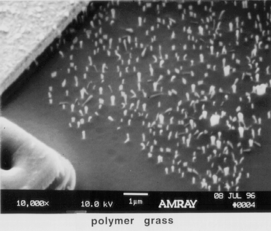
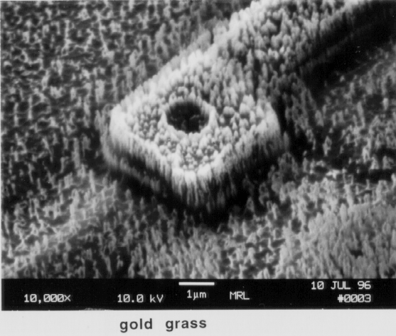
Sputtering gold during plasma etching is a common problem. The best solution is not to have any exposed gold on the sample by either removing it or masking it with Teflon or carbon blocks. If this is impractical, etching with as low power as possible will minimize the amount of gold sputtered.
Approach the correct etch time cautiously. It is better to have to put the sample back in the chamber and etch for a little longer than to destroy the sample by overetching it. Continue etching until the target layer is completely removed.
The amount of gold that is sputtered will depend on the power level chosen for the etch. If the gold cannot be removed or masked over, lower the etch power until the gold sputtering goes away (trial and error is always better on a test sample than on a real sample submitted for analysis). Sputtering will be machine dependent.
Two methods can determine the success of a buffered oxide etch. First, if a film thickness measurement system is available, use it before and after etching to determine the amount of material that has been removed. If a film thickness measurement system is not available, try to find an area where the passivation edge can be seen. One of the best places to look is the bond pads. During manufacturing, the bond pads are initially covered with passivation, in which a hole is opened to allow contact to be made to the metal. The edges of this hole are usually visible and make a good passivation etch removal monitor. Other lower oxide layers can be monitored by looking at the next material (poly, metal, or silicon) to be uncovered.
Keep repeating the etch until the layer to be removed is completely gone. As with all chemical etches, approach complete removal patiently, as repeated etches are always better than an overetched sample.
Barrel plasma etchers are notorious for undercutting metal during an oxide or nitride etch. Most wet chemical etches will also undercut and lift metal lines if the layer being removed is over etched. For either of these cases, approach the correct etch time slowly to avoid overetching.
Defects found under field oxide may or may not cause a problem unless the defect causes the region under the field oxide to turn on when a bias is applied to the conductors on top. Other conceivable defects may cause either a vertical short or a lateral conductive path bypassing the field oxide structure. Defects in the gate oxide region can almost always cause an electrical problem.
Using phosphoric acid to remove metal (Al) should only be done on structures that do not have silicon nitride (that is not to be removed) underneath. Otherwise, the only problem that may exist is overetching the top metal layer and subsequently removing a lower metal layer by acid passing through vias. However, this technique does decorate in-situ for via problems.
Hydrochloric acid will not etch non-metal layers. Although overetching is generally not a problem, overetching the top metal layer and subsequently removing a lower metal layer by acid passing through vias is a concern when removing the top metal layers. This technique also decorates in-situ for via problems. Be careful not to overetch the top metal layers and inadvertently etch the lower metal layers when the etchant passes through the vias.
Occasionally, the polysilicon can be easily removed by undercutting the oxide beneath it. If this is not your intention, look for any poly areas that seem to be out of place; this indicates that the etch has gone too long.
Sometimes, overetching the dielectric that covers the metal 1 will undercut the oxide underneath the metal and cause it to lift. Wet etches or barrel type plasma etchers are more prone to this than parallel plate plasma etchers. While inspecting the surface, look for features that appear to be in the wrong place, are at the wrong orientation, or are just missing. Always approach the correct etch time with caution and patience, as the etch can always be repeated again if it has not gone far enough.