System Maintenance occurs every Friday.
Optical Beam Induced Current (OBIC) is a scanning optical microscopy (SOM) imaging mode that localizes regions of Fermi level transition. OBIC is primarily used to localize buried diffusions and semiconductor defects. Minority carrier diffusion lengths and lifetimes have also been measured using OBIC, but these are very rarely applied during failure analysis. OBIC images are produced while monitoring the nonrandom recombination current of the electron-hole-pairs generated when an optical beam with photon energy greater than the smallest bandgap (indirect for Si and direct for GaAs) is scanned across a semiconductor. The recombination current may be increased or decreased by biasing the IC. Additional testing information can be useful in selecting the optimum conditions for performing OBIC. OBIC is an optical beam corollary to the Electron Beam Induced Current (EBIC) SEM technique.
OBIC imaging is performed if the location of diffusions (for example diode or transistor junctions) is desired. OBIC is particularly useful if the diffusion is buried below passivation. If metal conductors cover the area of interest or a flip-chip packaged IC is under examination, conventional optical microscopy is either difficult or impossible to implement for junction localization. OBIC can still be performed by using an infrared (IR) light source from the polished backside of the IC die. The energy of the IR source must be greater that the lowest energy bandgap of the semiconductor (~ 1.1 eV for the silicon indirect bandgap) to produce electron-hole-pairs. If lower energies (longer wavelengths) are used, then no electron-hole-pairs are produced and OBIC signal is not generated.
OBIC imaging is also useful in localizing semiconductor and junction defects such as stacking faults, dislocations, EOS/ESD damage, diffusion spikes, and diffusion pipes. These defects produce local variations in the Fermi levels or built-in potentials that can enhance or diminish the recombination current and hence the OBIC signal.
While the OBIC technique can be useful in localizing diffusions and semiconductor defects, three limitations hamper OBIC's effectiveness. First, only recombination currents relative to the test nodes selected are observed using OBIC. When an IC's power leads are used as test nodes, a large recombination current across a p-n junction connected to the IC's power leads through a complicated feedback network will not produce an OBIC signal if there is no charge flow relative to the power pins. The visibility of recombination currents deep inside IC logic can be increased by properly selecting which IC leads to use as test nodes, biasing the IC (and thereby "turning on" current paths to the IC's leads), and using small mechanical probes to access conductors connected directly to the junction(s) of interest. The ground and power leads of an IC are normally the initial test node choice for OBIC imaging of structures deep inside the IC because of their "global" nature, but other leads may be used if the IC's design or electrical testing suggest a better combination.
Second, while OBIC does not produce irradiation effects on ICs, the optical beam cannot penetrate through optically opaque layers. Backside OBIC using an appropriate IR laser is a solution to this problem, but this will require IC backside polishing to reduce light scattering. Third, even if no electrical or mechanical access limitations exist, the OBIC signal will normally include recombination current information from a majority of the diffusions on the IC using power and ground as test nodes. The additional information in the image can make it difficult to identify the site of a particular anomaly. Using light emission, liquid crystals, or another failure analysis technique to reduce the area for OBIC examination will reduce the amount of extra OBIC information and increase the likelihood of locating an OBIC defect.
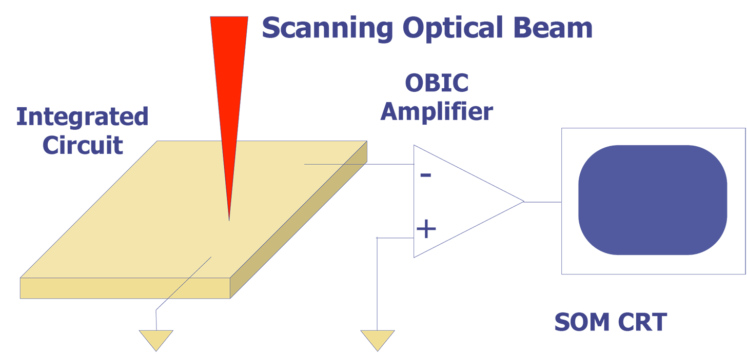
To obtain OBIC information, an optical beam (normally a laser) is scanned across an IC surface. When the optical beam with photon energy greater than the indirect bandgap for Si is scanned across a Si IC, absorption of the photon energy in the semiconductor will form electron-hole-pairs within the bulk of the IC. The relatively low ionization energies (less than 10 eV) of the materials used in IC manufacturing allow photon beams to produce many free electron-hole-pairs. These pairs usually recombine randomly in the material; however, if production occurs in a space-charge (depletion) region, the charge carriers will be separated by the junction potential before recombination, producing an OBIC current. Using an amplification configuration as shown in Figure 1, the recombination currents can be amplified and displayed on the SOM.


Usually the power and ground inputs are used as test nodes because of their global nature across the IC; however, other node combinations may be used if indicated by the failure history. The OBIC signal detector is the IC itself.
Since OBIC requires interaction between the photon beam and the junctions or defects of interest, optically opaque layers may be "probed through" by coming from the backside of a polished IC die using an IR light (laser) source. The wavelength of the light source must be chosen long enough to take advantage of the higher transmission of IR light in semiconductors but short enough (high enough energy) to produce electron-hole-pairs.
OBIC is performed to rectify defect localization. Biased OBIC can also yield the logic state of transistors under certain conditions. OBIC examination in itself is nondestructive, however the sample preparation must be done with care, especially if backside OBIC is to be performed. Backside OBIC requires IC polishing of the back surface to reduce scattering of the scanned IR light beam. Backside OBIC can eliminate the need for surface layer removal during failure site localization.