System Maintenance occurs every Friday.
System Maintenance occurs every Friday.
Electron beam microanalysis is a powerful analytical technique, capable of performing elemental analysis of microvolumes, typically spanning a few cubic microns in bulk samples and considerably less in thin sections. Analysis of X-rays emitted from a sample can be accomplished by energy dispersive spectrometers, which permit analysis by discriminating among X-ray energies. X-ray microanalyses permits identification and localization of elemental constituents on a sample, with resolution limits of 0.5 to 1.0 weight percent.
Energy Dispersive Spectrometry (EDS) was first introduced in the late 1960s, when solid state detectors were first interfaced to microanalyzers. Before that time, the wavelength-dispersive spectrometer (WDS) was used for x-ray characterization.
The concept behind wavelength-dispersive spectrometry is shown in Figure 1. An x-ray leaves the surface of the specimen and strikes the crystal. According to Bragg's law, the x-rays are reflected off the crystal into the proportional counter. The signal from the counter is amplified and converted to a pulse that enters the single-channel analyzer. This signal can then be counted with a scaler or sent to a computer for analysis. In practice, the crystal spectrometer readings are either proportional to wavelength or calibrated directly in wavelength. Tables or computer analysis can then be used to identify particular elements.


Wavelength-dispersive spectrometry uses Bragg's law to identify and separate x-ray peaks. A beam of coherent x-rays is assumed to be specularly reflected from the crystal planes, which are spaced d units apart. According to Figure 2, the lower of the two x-ray beams shown will travel an additional path length ABC = 2dsinθ prior to leaving the crystal. If that distance is an integral number of wavelengths, then the reflected beams combine in phase to produce an intensity maximum at the proportional counter. If the analyzing crystal is a high quality crystal, the full-width, half-maximum for a representative element is approximately 10 eV. X-rays that do not satisfy the Bragg criteria will be absorbed into the crystal or pass through it.


Most scanning electron microscopes equipped with WDS have more than one crystal (typically three or four). This allows examination of multiple elements and optimization of performance in different wavelength ranges. Some typical crystal materials include quartz, KAP, LiF, PbSt, PET and RAP.
The detector is typically a gas proportional counter. It consists of a gas-filled tube with a thin tungsten wire held at a 1-3 kV potential. The gas in the tube is typically an inert gas, such as argon or krypton, but occasionally mixtures are used, such as 90% argon - 10% methane. When an x-ray photon enters the tube and is absorbed by an atom of gas in the tube, the atom emits a photoelectron. Additional photoelectrons are generated as the initial electron collides with other atoms. The electrons are attracted to and captured by the tungsten wire. The number of photoelectrons generated depends on the energy of the x-ray photon. Detection can be optimized by varying the pressure of the gas, the applied voltage, and the temperature of the detector.
Because the crystals must be scanned slowly to create a WDS scan, the procedure can be quite time consuming. A typical WDS scan using three or four crystals might take between 20 minutes and one hour to complete. Because of this, EDS has become much more predominant for failure analysis applications. Still, WDS is able to resolve elemental peaks that are quite difficult to resolve using EDS.
In the late 1960s, Fitzgerald, Keil, and Heinrich first used the solid state detector as an electron beam microanalyzer. The detector resolution has now improved to the point where it is less than 150 eV. Because solid state detectors can gather data more quickly and are easier to manipulate, EDS has become the most commonly used microanalysis instrument that attaches to a scanning electron microscope. The basic design of an energy dispersive spectrometer is shown in Figure 3. The x-ray passes through a thin beryllium window into a cooled reverse-biased lithium-drifted silicon detector. Absorption of the x-ray photon in the detector generates a photoelectron, which in turn generates electron-hole pairs in the reverse-biased diode. These electron-hole pairs are swept away by the bias on the detector and are then converted into a voltage pulse by a charge sensing amplifier. The signal is further amplified and sent to a multichannel analyzer, where the pulses are sorted by voltage. The distribution by voltage can then be displayed and manipulated by the computer to identify peaks or quantification.


Several issues can perturb an EDS spectrum, including peak broadening, peak distortion, silicon x-ray escape peaks, absorption edges, and the silicon internal fluorescence peak. In addition, several hardware-related problems, such as pulse pileup rejection by the main amplifier, acoustic coupling on the co-axial connector between the detector and the amplifier, ground loops, and ice in the detector system, can occur.
Peak broadening results from statistical variations in the number of charge carriers and thermal noise in the amplification process. While the natural width of an x-ray peak might be on the order of 0.04% of the peak energy, the statistical and thermal artifacts increase this width to around 0.1% of the peak energy. The only method for reducing this problem is to increase the number of counts in the spectrum.
Peak distortion is caused by non-uniform regions of the detector near the faces and sides. Traps and recombination sites result in recombination of electron-hole pairs, thus distorting the output. In addition, a phenomenon known as the background shelf will increase the background at the energies below a peak. This can be quite noticeable with a strong peak. This is caused by continuum x-ray being inelastically scattered from the detector, which reduces the number of charge carriers collected. This results in more lower energy counts and fewer higher energy counts.
Silicon x-ray escape peaks result from interactions with the detector that leave a silicon atom in an ionized state. An auger electron can result as an electron moves to fill the vacancy. Since the emitted auger electron will only travel a fraction of a micrometer, it will recombine in the detector, contributing to the charge carrier process. However, some fraction of these electrons do indeed escape; therefore, they do not contribute to the creation of electron-hole pairs. This phenomenon creates an "escape peak" equal to the energy of the parent line minus the energy of the silicon x-ray. Since the silicon Kα peak is about 50 times stronger than the Si Kβ peak, only the Si Kα peak is normally observed. The magnitude of the escape peak can vary from approximately 2% in phosphorus to 0.01% in zinc.
An absorption edge arises from the protective window of beryllium, the gold coating on the detector, and the inactive layer of silicon on the detector. Some x-rays are absorbed by these materials before entering the active portion of the detector. The beryllium window essentially eliminates all x-ray energies below 600 eV. Virtually all x-rays above 2 keV pass through the window. The change in the x-ray continuum takes place at the absorption edge of silicon and, to a lesser extent, at the absorption edge of gold. This creates a small step in the continuum.
The silicon internal fluorescence peak is caused by the emission of Si Kα x-rays from the inactive silicon layer. Some of these x-rays make their way into the active region of the detector and create a small silicon peak. This peak normally causes an apparent concentration of 0.2 wt% or less silicon in the specimen.
In order to achieve maximum energy resolution, the amplifier must have sufficient time to recover after processing each signal. The use of a long time constant can result in a second pulse arriving at the amplifier before the first pulse is completely processed. This problem results in the need for pulse pileup rejection. When two pulses arrive close together, a peak at double the energy or at a sum of the energies can result. The pulse pileup rejection circuitry cannot eliminate this problem, but it can reduce it substantially.
Acoustic interference can cause an extremely high background count for low energies (from 2 keV down to 0 keV). This is the result of noise coupling into the amplifier from the wire between the detector and the amplifier. Because this length of wire can act as a very sensitive microphone, it must be shielded adequately from mechanical vibrations.
Ground loops can cause distorted spectra by introducing 60 Hz noise and other signals into the detection electronics. Because the EDS signals are very low level signals, the metal components of the system must be adequately grounded so that no potential difference can exist. Voltage differences on the order of microvolts can cause problems that introduce noise into the EDS spectra.
Finally, ice accumulation in the detector causes vibrations that potentially degrade the resolution of the system. Small particles of ice or water droplets can move about in the detector during boiling of the liquid nitrogen. This vibration can be transmitted to the detector. An accumulation of ice at the bottom of the detector raises the temperature of the detector and increases the thermal noise component; both these factors degrade the resolution.
With the advent of microcomputers to analyze x-rays, quantitative x-ray analysis has become possible. Although EDS systems are relatively good at identifying elements in samples, the accuracy of quantitative x-ray analysis depends on the standards and the operating conditions of the SEM. A rough rule of thumb would be that quantitative analysis is accurate to about 1% with standards and to about 5% without standards.
The most commonly used quantitative analysis technique is the ZAF technique. In the early 1950s, Castaing showed that the average number of ionizations, n, from element i generated in the sample per primary beam electron incident with energy E0 is


where dE / dX is the mean energy change of an electron in traveling a distance dX in the sample, N0 is Avogadro's number, ρ is the density of the material, Ai is the atomic weight of i, Ci is the concentration of element i, EC is the critical excitation energy for the characteristic x-ray line of interest , and Q is the ionization cross section, defined as the probability per unit path length of an electron of given energy causing ionization of a particular electron shell of an atom in the specimen. Knowing the measured intensity from a sample and a standard allows the analyst to calculate Ci (the concentration of the element in the sample) directly using the ZAF factor, where Ci = (ZAF)iki
Zi is the atomic number effect, Ai is the absorption of x-rays within the specimen and Fi is the fluorescence effect for each element. The three correction factors each play a part in determining the true quantitative amount of the element present in the sample.
The absorption factor arises from some of the x-rays becoming absorbed in the specimen, thus not leaving the sample and entering the detector. This results in a decreased magnitude of the intensity of the x-rays reaching the detector. The three major factors that influence the absorption factor are the operating voltage of the scanning electron microscope, the take-off angle of the electrons, and the mass absorption factor for the element of interest.
The atomic number effect comes from two phenomena: electron backscattering and electron retardation. This effect, if unaccounted for, causes heavy elements in a light element matrix to yield values that are too low, while light elements in a heavy matrix yield values that are too high. Duncumb and Reed developed a formulation by which the atomic number effect can be determined. The atomic number effect, Zi, is given by


where Ri and R'i are the backscattering correction factors of element i for standard and specimen respectively.
Finally, the characteristic fluorescence correction arises when the energy E of a characteristic x-ray peak from element j is greater than the critical excitation energy EC of element i. The correction is necessary because the energy of the x-ray peak from element j is sufficient to excite x-rays secondarily from element i. Because the x-ray fluorescence always adds intensity for element i, an equation to calculate the fluorescence can be expressed as follows:


The correction factor Ifij/Ii relates the intensity of radiation of element i produced by fluorescence to element j. Reed developed the most commonly used correction factors for fluorescence. This fluorescence factor is usually the least important factor in the ZAF correction.
There are several reasons why one should consider EDS for microanalysis: ease of acquisition, cost-effectiveness, and technique prevalence.
For standard integrated circuit technologies, X-ray analysis can easily identify major elemental constituents on or near the surface and/or surface contaminants of several weight percent. With a 40 keV primary electron beam, the penetration depth is approximately 10 microns. The depth at which the primary electrons have sufficient energy to generate characteristic X-rays is somewhat less than this, approximately half. Detection limits also apply to small atomic number elements. Boron is usually the smallest element that can be detected by X-ray analysis; however, this lower limit depends on the type of detector being used.
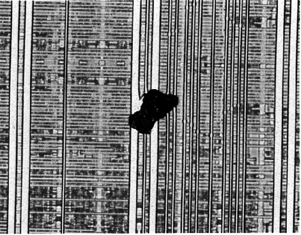
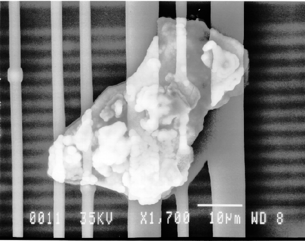
If any particulates are observed in the area of interest, one would employ the EDS system to identify the constituents of the particles.
Characteristic X-rays are generated from electron beam interaction with the sample volume. When the electron beam displaces an inner core electron, an electron from a higher energy level will decay to replace the missing inner electron. The transition from the higher energy level to the lower level will be accompanied by an energy release, whose magnitude is the difference between the two electron energy levels. A photon (X-ray) with this "characteristic" energy is one form of energy release. Because the inner core electrons of different atoms are separated by known, discrete energy levels, elemental identification is possible from observing the energies of the characteristic X-rays produced.
In order to collect a spectrum, select the area or point of interest using a beam energy of approximately two and one-half times the highest energy X-ray line to be excited. Select the auto identification program and identify the major and minor peaks of the collected spectrum. All peaks should be accounted for. The spectrum can either be stored or printed out depending on the analyst's need. Peaks can also be identified by employing the cursor to find the peak energies and using a X-ray energies chart to identify the peaks.
If the particles are less than 10 microns, the analyst can attempt several techniques. A specimen tilt angle towards the detector can provide more particle area to the electron beam, and lower beam energies can be used for less electron beam penetration into or through the particle. If the substrate material is excited, the identification of the elemental constituents of the particle is more complicated. However, the beam energy must be 2 to 2.5 times higher than the x-ray energies of the elements to be detected. Figure 3 shows an example of an EDS spectrum on a particle found on an IC. Notice that although the energy extends to 20 keV, no peaks are visible beyond about 10 keV.


Energy dispersive spectrometry can be performed on a particle whenever any questions arise about the elemental constituents of the particle. With the identification of the elemental make up of the particle, the origin of the particle is sometimes easily obtained.