System Maintenance occurs every Friday.
Electro-optic probing is a class of techniques which relies on the detection of changes in the polarization of an optical beam probe to measure voltage waveforms. Because of the nature of the polarization changes, very high frequency signals can be measured accurately without loading on the circuit.
In 1875, a physicist named Jon Kerr discovered that an isotropic transparent crystal becomes birefringent when placed in an electric field E. It takes on the characteristics of a uniaxial crystal whose optic axis corresponds to the direction of the applied field. The two indices, n-parallel and n-perpendicular, are associated with the plane of vibration of the wave. Their difference, Dn, is the birefringence given by
Dn = loKE2
where lo is the wavelength of the light, E is the applied electric field, and K is the Kerr constant. Materials which exhibit the Kerr effect are usually polar liquids such as benzene, chloroform, and water.
In 1893, another physicist named Friedrich Pockels discovered that a similar electro-optic effect occurred in certain types of crystals. However, as opposed to the Kerr effect, the birefringence of the Pockels effect was linearly proportional to the applied electric field. Crystals which show this effect lack a center of symmetry. Of the thirty-two crystal symmetries, twenty are suitable for this effect (these crystals were also piezoelectric). This relationship between crystal structure and Pockels effect excluded many crystals and all liquids. Common crystals for this purpose include lithium niobate (LiNbO3) and potassium dideuterium phosphate (KD*P).
In 1972, D. Auston and his associates first reported the use of the electro-optic effect for measurement of electrical signals. Since that time, researchers have developed and refined three major methods for performing electro-optic probing: a direct method for GaAs (using the material itself as the probe), an indirect method (using LiNbO3, KD*P or other materials) for both GaAs and Si devices, and a variant which utilizes charge carrier density fluctuations in Si. Engineers have also developed sampling methods to improve voltage and waveform accuracy. In several years, commercial hardware for electro-optic waveform measurement will likely become available.
The retardation of the cell is usually given as a phase change, Df, where a value of Df = p is coincident with the half wave voltage, Vl/2. This retardation of the light as it passes through the Pockels cell makes these materials suitable for the measurement of electric fields in semiconductor devices. Theoretically, the response time of these materials is fast enough to measure high frequency events.
The Pockels effect can be applied to the measurement of high frequency events in microelectronic devices via internal or external (or direct and indirect) methods. Figure 1 illustrates the relationship between these concepts.


The indirect measurement method places one of the known Pockels crystals (typically KD*P or LiNbO3) in close proximity to the areas of interest on the top side of the integrated circuit. Typically a non-contact, non-destructive measurement, this method requires no further sample preparation after the IC surface is exposed. The direct measurement uses the semiconductor substrate as the electro-optic material. In this case, the electro-optic effect will be smaller than in the crystals listed above. However, the measurement uses fields present in the IC substrate rather than requiring the fields to affect the optical properties of a crystal held in close proximity to the IC.
Direct electro-optic techniques cannot be used on silicon-based devices, making indirect electro-optic techniques from the front side of the IC the only viable method. However, Heinrich et. al. have demonstrated that free carriers in an active device perturb the local index of refraction and absorption coefficient. The absorption coefficient change is small in the near infrared (that is necessary for backside probing), but the changes in the index of refraction are large enough for detection. This allows for a direct "electro-optic like" technique from the backside. The basic setup for this technique is shown in Figure 3. A lack of useful waveform acquisition techniques from the backside of a silicon IC has created considerable interest in commercializing this technique.
Electro-optic probing is a newer technique that enables the acquisition of waveform information from an IC when nodes of interest are difficult to access from the die frontside. Because of its high bandwidth, electro-optic probing is also quite useful for acquiring waveforms from high frequency technologies or components, such as GaAs ICs and MIMCs. Another reason to consider electro-optic probing is its ability in certain instances to capture single shot waveforms. This can eliminate the need for a repetitive pattern and sampling.
Because electro-optic probing is still in its infancy, no commercial systems are currently available. In order to be useful in most failure analysis laboratories, electro-optic probing necessitates substantial investment in personnel with specialized knowledge of the physics of materials, optics, and integrated circuit behavior. Therefore, electro-optic probing should only be considered if the advantages of the technique outweigh the cost and resources required to set it up.
Hardware
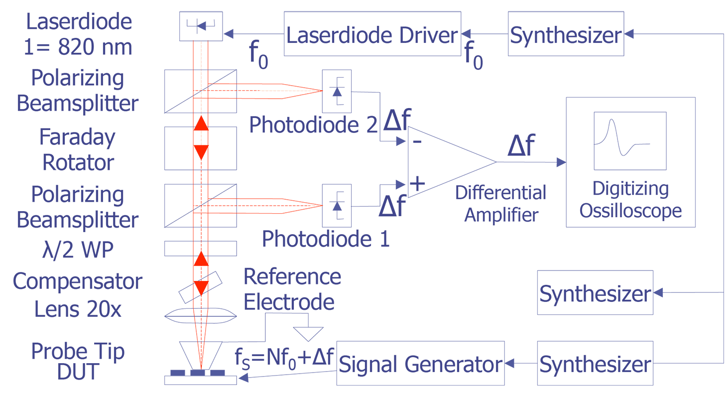
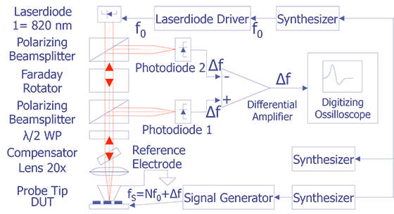
Electro-optic probe hardware is comprised of several elements: 1. an appropriate laser or laser diode, 2. an electro-optic crystal (if using an external crystal for detection), 3. detectors for sensing the phase shift of the laser beam (typically photodiodes), 4. a variety of optical hardware, including polarizing beam splitters, magnifying lenses, a faraday rotator, and a half-wavelength waveplate, and 5. detection electronics. Two basic electro-optic configurations exist: one for an indirect measurement and one for a direct measurement. The indirect system uses an external electro-optic crystal, such as lithium niobate or potassium dideuterium phosphate. The direct system uses the semiconductor material as the electro-optic element. Gallium arsenide can be used directly, while changes in the charge density allow measurements to be made in silicon materials.
Figures 2 and 3 illustrate these two basic systems. In Figure 2, the indirect optical configuration is shown. Light generated from a laser diode passes through a polarizing beam splitter, a Faraday rotator, a second polarizing beam splitter, a half-wavelength waveplate, and a compensator, where it is magnified before entering the electro-optic probe. The light reflects off the sample surface. In Figure 3, light travels from the laser through the two polarizing beam splitters and the Faraday rotator to the half-wavelength waveplate. The custom Nomarski prism splits the light into two beams. On the backside of the IC, the light is magnified and focused. Finally, the reflected signals are captured by the two beam splitters and detected by two photodiodes to form the signal.


Electro-optic probing is usually performed to acquire waveforms on an IC. The technique is very similar to electron beam probing. Because electro-optic probing is still mainly a research tool, expect setup and acquisition times to be fairly lengthy. Furthermore, because fault isolation using backtracing of waveforms is time consuming, the technique should be performed after rapid localization techniques have been tried.
One feature that makes electro-optic probing very attractive as a failure analysis technique is the fact that it is a non-destructive technique. However, the sample may need to be prepared for the direct electro-optic technique (the backside of the die must be exposed and in a condition such that infrared light can reach the circuitry of interest). Consequently, electro-optic probing should be performed immediately after rapid localization techniques. If you have electron beam capability to probe the IC and the signals can be adequately sampled using e-beam techniques, use electron beam probing. If the signals to be probed cannot be properly sampled using e-beam techniques (high frequency, low duty cycle, single shot event), try electro-optic techniques.


