System Maintenance occurs every Friday.
System Maintenance occurs every Friday.
Lasers have been used for many years to alter or isolate conductors on integrated circuits. Systems designed for this purpose work on the principle that laser light (generally from a pulsed laser) when focused through microscope optics can selectively remove material from an IC without otherwise damaging it. If done properly, lasers can be used to cut or remove metal lines, open holes in some types of passivations, or cut polysilicon conductors on ICs. If done improperly, material from the conductor being cut can be moved into insulating layers, causing shorts.
Three predominant laser types can be used for laser cutting. In the infrared wavelengths, Nd:YAG (Neodymium Yttrium Aluminum Garnet) lasers operating at a frequency of 1064 nm are the most common. In the visible wavelengths (green), two major types of lasers are most commonly used: the frequency doubled Nd:YAG laser at 532 nm and the Xenon gas laser operating at a wavelength of 500 nm with a pulsed power output of about 150 µJ.
The first YAG lasers designed for silicon surgery were infrared (IR) lasers operating at a wavelength of 1064 nm, or in the IR range. This is the fundamental frequency of Nd:YAG lasers, which are used in many applications in conjunction with IR-specific microscopes. IR lasers have several limitations. Most materials used in the fabrication of integrated circuits (ICs) absorb energy more efficiently at shorter wavelengths than those produced by IR lasers. This means much more power is required to do the same job as compared to using a laser with a shorter wavelength. This excess energy often results in unnecessary damage to areas adjacent to the area of interest. As mentioned above, the IR YAG laser works only with microscopes designed specifically for IR wavelengths. By contrast, most microscopes used in failure analysis are usable only in the visible spectrum. Using a YAG laser with a non-YAG microscope will likely result in burning some part of the microscope optics. Also, using a non-YAG microscope results in a large reduction in energy relative to that available with a YAG-compatible microscope. Another disadvantage of IR lasers in silicon microsurgery is that cut sizes are limited to a minimum of about 2µm x 2 µm because of the longer wavelength.
Today, most suppliers and failure analysts use "green" wavelength lasers, such as the frequency doubled Nd:YAG laser or Xenon gas laser. Most metals used in ICs (aluminum, gold, titanium-tungsten, etc.) absorb more green light than IR wavelength energy, thus requiring less energy to perform a specific job. As mentioned above, lower energy is preferred because less damage occurs in adjacent areas. Green lasers are also well suited for the standard visible-light microscope optics most commonly used in failure analysis. The minimum spot size for green lasers is approximately 1µm x 1 µm.
Several lasers produce energy in the ultraviolet (UV) range, including frequency tripled or quadrupled Nd:YAG lasers and excimer lasers (XeCl, XeFl, etc.). The ultraviolet range begins just below the visible spectrum, or less than 400 nm. Ultraviolet lasers have an advantage over IR and green lasers because most passivation materials absorb more UV energy than either IR or visible energy. Therefore, an even smaller amount of UV energy is necessary to directly remove passivation. With the IR or visible lasers, passivation is removed indirectly by heating the material beneath and "blowing off" the passivation from the heat generated by the underlying metal. UV lasers are able to remove passivation directly because most passivation materials absorb UV energy directly.
However, UV lasers have a microscope-related problem that is similar to the one encountered when using IR lasers. The difference is that UV lasers operate at the opposite end of the visible spectrum from IR lasers. Since UV laser energy is below 400 nm, the optics in most microscopes used in failure analysis (designed for visible light, 400 - 700 nm) will not pass the shorter-wavelength UV energy. If one can solve the microscope problems of non-UV transmitting optics, one would find some help with objective lenses. Some types of microscope objectives, called reflecting objectives, will work in the UV spectrum. Unfortunately, image quality of a reflecting objective is much poorer than that of standard failure analysis microscope objectives. Additionally, reflecting objectives are available in a limited number of magnifications; the most common for laser use are 36x and 52x. This makes them suitable only for removing relatively large areas of passivation and cutting rather large lines. However, as microscope technology improves in the UV wavelength, UV will become an excellent alternative for failure analysis because of effective energy absorption of most passivation materials, improved cutting depth control and potentially sub-micron cut sizes.
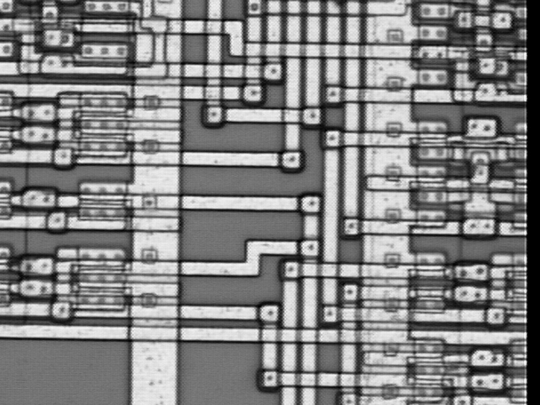
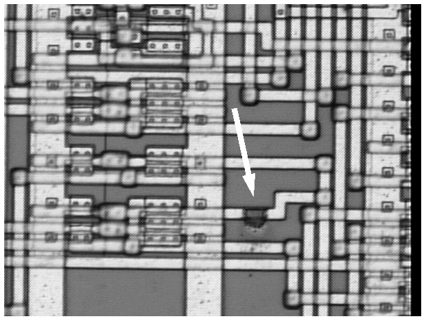
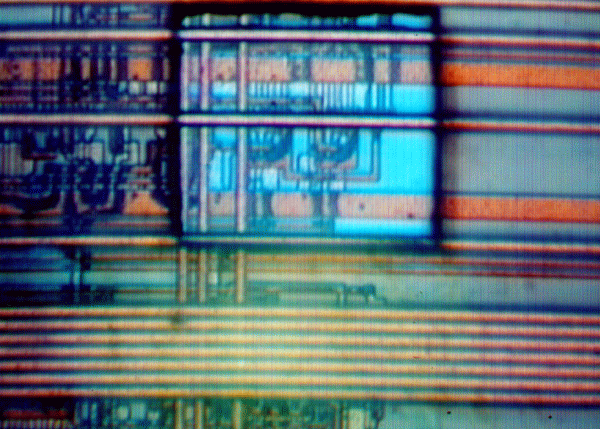
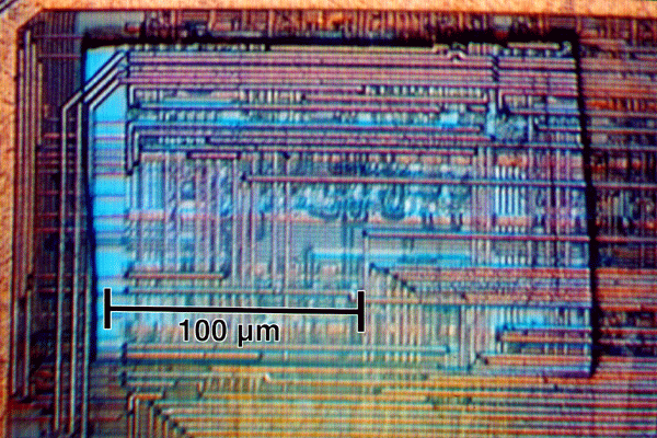
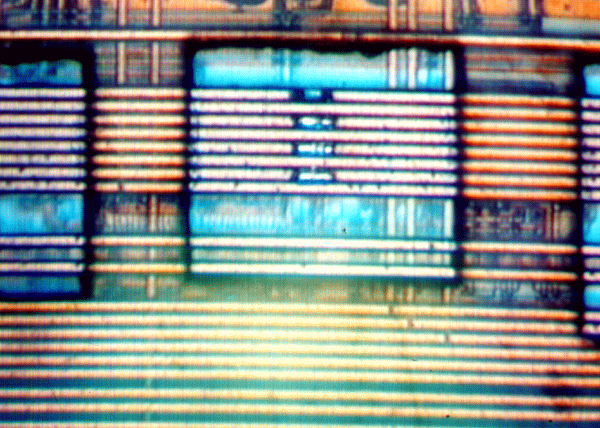
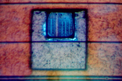
As an example, Figure 2 and Figure 3 show a metal line before and after being cut by a Xenon laser system. In this case, the apertures on the laser were set to cut one line and leave the lines around it unaffected. Although selecting the appropriate power level to use must be done through a trial and error process, care must be taken to avoid using too much power, as this can move metal into insulating layers and cause shorts.
Laser cuts can be made for many different reasons and in many different types of materials. Lasers have been used for two purposes: selective layer removal and interconnect isolation. Many types of IC failures can be identified if the problem section can be electrically removed from the rest of the IC and studied by itself. Often, when the circuit is intact, the available electrical information can be difficult to interpret. For example, if a gate oxide rupture has occurred on an IC, the circuit will not behave functionally as intended. When the bad transistor is activated, the IC will draw excess current. A series of laser cuts can isolate the faulty transistor from the remainder of the IC. Once isolated, microprobes can be used to measure the I-V characteristics of the transistor by itself. This type of analysis can prove that the transistor in question was at fault.
The above example assumed that the passivation of the IC had been removed prior to microprobing. In some cases, the laser can be user successfully to remove passivation over conductors to allow probing. Silicon nitride passivation can be readily removed over aluminum with a Xenon laser. Silicon dioxide and silicon oxynitride can be removed, but with some difficulty. The use of different wavelengths of lasers could make selective removal of oxides easier.
The use of a laser cutter is very straightforward. Once the procedure to be accomplished has been selected, whether it is selective material removal or isolation of conductors, it is best to experiment with laser power level either on an unimportant area of the IC or on a second IC of the same technology. It is best to start with a low laser power and gradually increase the power until the desired result is obtained. When opening holes in passivation, increase the power until the hole is opened, but the metal underneath is not disturbed. When isolating metal lines, use the lowest power that completely cuts the line in a single laser pulse. Each time the power level is changed, move the sample to a fresh spot before firing the laser. This will ensure that materials have not been altered by a previous laser pulse.
If the line is still partly intact, increase the power level and try to cut the line again. Repeat this procedure until the line has been fully isolated. It is always best to try to obtain the correct power level on a test sample if possible. If a test sample is not available, try to find a representative area on the IC that is not used, i.e. test transistors on the die or in the saw apart areas left on the edges of the die.
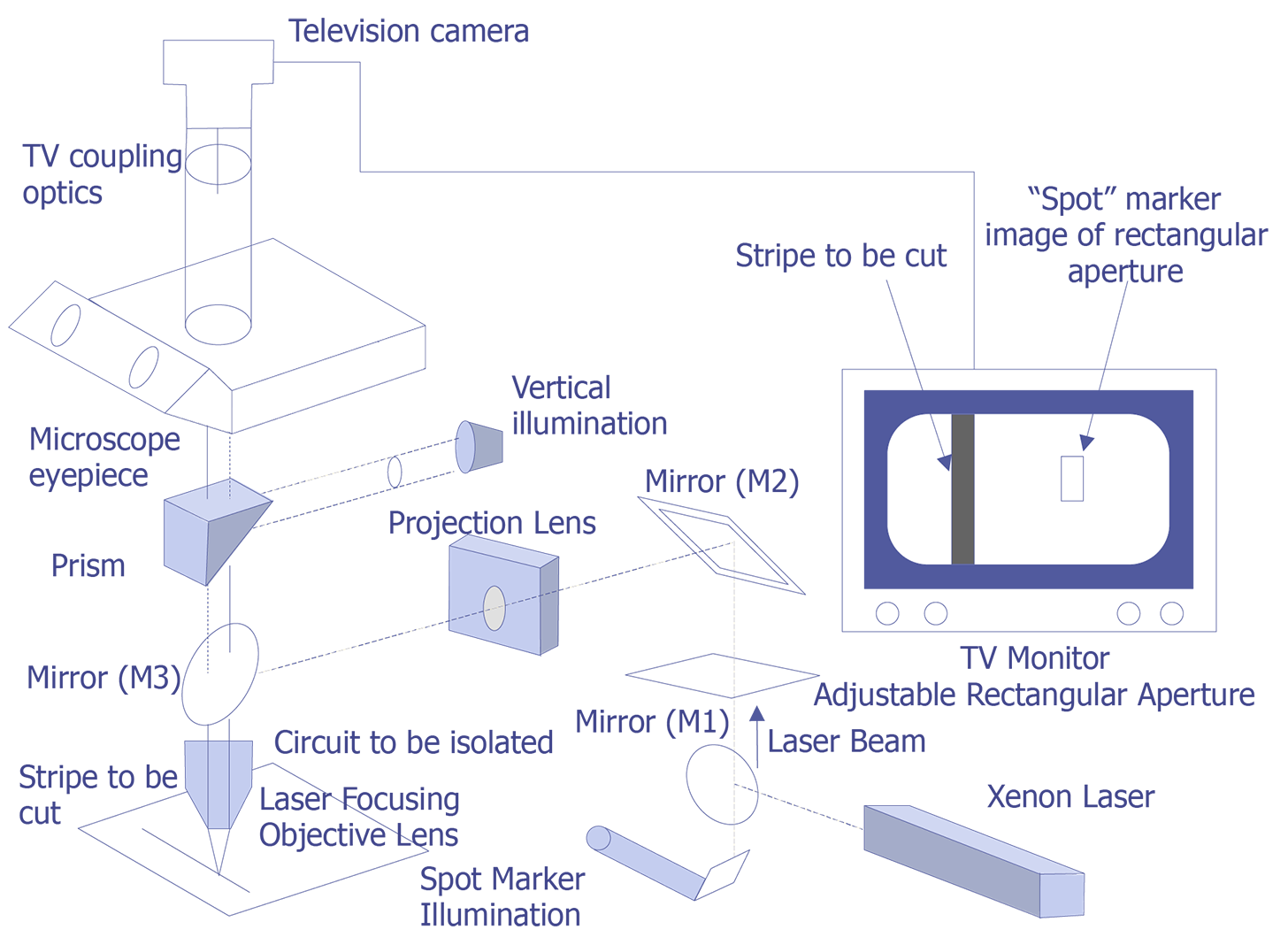
If other circuitry was damaged, one of three problems has occurred. First, too much power may have been used. Try reducing the power and determining if the line has been completely cut. Second, the laser may not have focused to the correct spot. Some laser cutters have a marker that is visible through the eyepieces that shows the location and shape of the area to be lasered. Other systems rely on marker superimposed on a TV image of the field of view. When using these systems, a cut is made in a test area and the markers are moved to the spot where the laser beam hit the sample. Lastly, some systems allow the user to adjust the length and width of the laser cut to be made by adjusting several apertures. Use these apertures to constrain the beam further so that the neighboring circuits are not hit by the beam.
In most cases, the laser will fail to cut the line until a threshold power level is reached. Most systems will not show a gradual increase in the amount of cutting with power level.
To answer this question, some information about your microscope and your sample device is necessary.
The most effective objectives for cutting and passivation removal are the 50x, 80x, and 100x objectives. Very little cutting can be done with lower power objectives because insufficient energy density is focused to the sample. While the total energy through each objective for a given energy setting is nearly the same, the energy density changes dramatically. Specifically, density changes with the square of the magnification change. This is because the laser energy is effectively "focused" by the higher power objectives. Table 1 shows this relationship using a 50x objective as a reference.
| Objective Lens | (= a) | Magnification Factor | (vs 50x lens = a/50) | Energy Density Factor | (vs 50x lens = a2/502) |
|---|---|---|
| 10x | 10/50 = 0.2 | 100/2500 = 0.04 |
| 20x | 20/50 = 0.4 | 400/2500 = 0.16 |
| 50x (reference) | 50/50 = 1.0 | 2500/2500 = 1.0 |
| 80x | 80/50 = 1.3 | 6400/2500 = 2.56 |
| 100x | 100/50 = 2.0 | 10000/2500 = 4.0 |
If a 50x objective is required to generate adequate energy density for most laser cutting tasks, it is obvious from the table that very little can be done with 10x and 20x objectives. It is also obvious how cutting power increases dramatically when moving to an 80x or 100x objective. The same task requires less power to accomplish with the 80x or 100x objective than with the 50x objective.
Most passivation materials absorb less visible laser energy than metal lines absorb. Thus, effective removal of passivation requires higher energy than is required to remove a metal line of equal size. If a part does not have passivation and you assume it does, the first laser pulse may cut the line and damage the substrate below. Figure 1 shows the absorption coefficient for aluminum and gold.


Different types of passivation require different energy levels. Oxide and nitride require less energy to remove than polyimide. For example, with a 50x objective, it might take 50% of maximum emergy to remove oxide or nitride and 75% to remove polyimide. Since heat generated by the metal below is being used to "blow off" the passivation, success will depend to some extent on the amount of metal being heated. It will be much easier to remove polyimide from a large metal area than from a small metal area since the larger metal area will be able to absorb more energy without damage. In general, it is easier to remove passivation from a line by making the laser aperature spot marker a long rectangle along the length of the line. Also, results will be better when removing passivation with an 80x or 100x objective than with a 50x objective.
It takes a higher energy level to remove a large area of material than it takes to remove a small area of the same material. Since the energy density remains constant as the laser aperture opens, one would expect that the energy density required to remove a small line would also apply to a larger line. However, metal is an excellent heat conductor and some energy placed in the target area is dissipated into the surrounding areas. The net result is that removing a large area of material requires a higher energy density than removing a small area.
A practical application of this phenomenon can be seen when faced with having to cut a large line or a bus. If the bus is too long to be cut in one shot, one might try either: a) making a long, narrow (2 - 3 µm) cut or b) using the nibble technique, i.e., make several smaller cuts 5 - 10 µm in length.
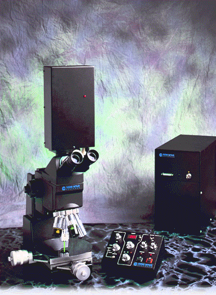
At some point, you may be faced with using a laser for the first time or a chip of unknown origin. Where do you start to remove passivation or make a cut? The bracketing technique, which starts at a very low energy and works up to the target, is the first recommended step in the process. The following example uses the New Wave Research LCS-1 Laser Cutting System. With a 50x objective, start with the energy switch in the high position, and the attenuator set at 300 and try a shot in a test area. If a setting of 300 did not produce enough energy, set the attenuator to 400, select a new location and try another shot. For best results, each new test shot would be at a new location. If 400 is too low to achieve the desired results, increase the energy to 500, then 600, etc., until too high an energy level is reached. Then, drop back 50 points, i.e., from 600 to 550, and try another shot. If that is still too high, drop back another 25 points to 525. Most materials have a large damage threshold. Following this procedure, you may notice some material removal at 400, and a little more at 500, and finally the desired results at 600.
A few materials have a small or narrow damage threshold. Thin film resistors and very small lines fall in this category. You might find that 200 is inadequate and 300 is too high. In this case you may have better results by moving the energy switch to the "low" position. This has the effect of reducing the energy level by 50% for a given attenuator setting. What this means is that you may now have to move the attenuator to 400 or 450 to get the same results you obtained at 200.
The high/low energy switch gives you a greater dynamic range, which is especially helpful for very low energy applications such as thin film resistor trimming. The attenuator will give you an attenuation of > 50:1; with the High/Low switch this becomes > 100:1. This switch is also a very handy feature for reducing the energy level quickly. For example, after removing passivation with the energy switch in the High position, use the Low position to remove the metal line beneath or to clean up a cut.
As noted above, multiple shots may be necessary to gain the desired result. Sometimes two shots at the same energy setting may be necessary. Other applications may require one high shot to remove passivation, as described in the above example, and a second lower energy shot to cut a line. If a single shot doesn't accomplish your task, try variations of multiple shots.
This represents just some of the characteristics of lasers and application techniques applied to silicon microsurgery. Laser and microscope technologies are expanding and improving rapidly. The most important improvements are higher power objectives with adequate working distance that will allow surgery on smaller geometries and UV optics that will allow UV to be used for passivation removal with greater depth control.
The following table summarizes the optimum wavelenght(s) recommended for common semiconductor materials. Table 3 lists recommended setting for removing passivation over the top metal layer. After passivation is removed, use 1 or 2 additional shots with green (532 nm) at the setting used to remove oxide passivation.
| 1064 nm (infrared) | 532 nm (green) | 355 nm (ultraviolet) | |
|---|---|---|---|
| Dielectrics | Silicon Dioxide | Nitride | |
| Nitride | Polyimide | ||
| Polyimide (big cuts) | Teflon | ||
| SOG (spin on glass) | Silox | ||
| Interconnect | Aluminum | Polysilicon | Gold (pulsed cut) |
| Gold | Aluminum | ||
| Aluminum | |||
| Tungsten | |||
| Copper | |||
| Thick and thin film resistors |
| Sample | Cut Size | Microscope Objective Lens | Wavelength | Energy Setting | Energy Range | Shots |
|---|---|---|---|---|---|---|
| Polyimide | 40 x 40 µm | 50x NUV | 355 nm | 200 | Lo | 75 |
| Si3N4 | 40 x 40 µm | 50x NUV | 355 nm | 300 | Lo | 40 |
| Si3N4 | 4 x 4 µm | 50x NUV | 532 nm | 500 | Hi | 2 |
| SiO2 | 2 x 4 µm | 50x NUV | 532 nm | 500 | Hi | 1 |
| SiO2 | 2 x 4 µm | 100x | 532 nm | 200 | Hi | 1 |
| SiO2 | 1.8 x 3 µm | 50x NUV | 532 nm | 400 | Hi | 1 |
| SiO2 | 1.8 x 3 µm | 100x | 532 nm | 200 | Hi | 1 |
| SiO2 | 2 x 4 µm | 50x NUV | 532 nm | 350 | Hi | 2 |
| SiO2 | 2 x 4 µm | 100x | 532 nm | 200 | Hi | 1 |
| Si3N4 & SiO2 | 2 x 4 µm | 50x NUV | 355 nm | 600 | Lo | 5 |
| Si3N4 & SiO2 | 2 x 4 µm | 50x NUV | 355 nm | 400 | Hi | 3 |
| Si3N4 & SiO2 | 1 x 2 µm | 100x NUV | 355 nm | 350 | Hi | 3 |
| Si3N4 & SiO2 | 20 x 4 µm | 50x NUV | 355 nm | 300 | Lo | 20 |
| Si3N4 & SiO2 | 20 x 4 µm | 50x NUV | 355 nm | 300 | Hi | 2 |
| Si3N4 & SiO2 | 2 x 4 µm | 100x NUV | 355 nm | 150 | Lo | 15 |
| Si3N4 & SiO2 | 2 x 4 µm | 100x NUV | 355 nm | 350 | Hi | 2 |
If the top passivation layer is nitride or polyimide, remove it using the settings noted in Table 3 above. Next, change to the 100x objective lens and use a single shot of green (532 nm energy) and a setting of 500, Hi to remove the next layer of oxide (if it is present) and then a second shot at the same energy setting to remove the top layer of metal. The next layer of metal (if it exists) may also be removed using one shot to remove the interlayer dielectric and a second shot to remove the next metal layer. It is best to reduce the aperature when removing the second metal layer to minimize the possibility of shorting between layers.
Laser cuts are used for two distinct purposes: opening holes in passivation and isolating conductors on ICs. Once other non-destructive diagnostic techniques have been used to characterize the fault, destructive techniques can help fully understand the electrical signature of the fault on the IC. In some cases, a processing or mask defect can deposit a conductor in an unintended location. For these cases, a laser cutter can be used to prove that the IC will be fully functional after the correction has been made. It is always cheaper to laser cut material from a few non-functional ICs to prove that a mask change will correct a problem than to make a new mask and fabricate a wafer lot without solving the problem. Laser cutters, or equivalently focused ion beam systems, are invaluable for these applications.