System Maintenance occurs every Friday.
System Maintenance occurs every Friday.
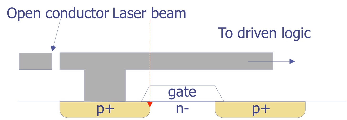
Light Induced Voltage Alteration (LIVA) is a scanning optical microscopy (SOM) imaging mode that localizes junctions connected to floating conductors. LIVA is an optical beam corollary to the Charge Induced Voltage Alteration (CIVA) SEM technique.
LIVA should not be confused with OBIC (Optical Beam Induced Current). The LIVA signal is derived from the voltage fluctuations on a power supply, whereas the OBIC signal is generated by current flow at a specific junction on the IC (see Figure 1)

LIVA imaging is performed to rapidly locate open interconnections that are connected to a diffusion. LIVA is particularly useful for imaging C4 (controlled collapse chip connect) technologies or ICs with dense metal interconnect where imaging from the back side of the die is more useful. This technique can be used to compliment other backside FA techniques such as OBIC and Light Emission.
While the LIVA technique can be useful in localizing open interconnect defects, three factors limit its effectiveness. First, only recombination currents relative to connected junctions are observed using LIVA. The LIVA technique cannot be used to image open interconnects that are open without a connected diffusion. Second, while LIVA does not produce irradiation effects on ICs, the optical beam cannot penetrate through optically opaque layers. Backside LIVA using an appropriate IR laser is a solution to this problem, but this solution requires IC backside polishing to reduce light scattering. Third, even if there are no electrical or mechanical access limitations, the LIVA signal will normally include recombination current information from other diffusions on the IC that are connected to high impedance nodes within the circuit such as multiplexers or tri-state bus lines. The additional information in the image can make it difficult to identify a particular anomaly.
It is critical to develop new failure analysis techniques to keep pace with the continued development of increasingly complex ICs. These new, improved analysis techniques should be easier to use, less damaging, more sensitive, and provide better spatial resolution. This challenge is being met with advanced techniques, including those that can be broadly categorized as either "passive" or "active." Passive techniques are noninvasive in the sense that the normal operation of the IC provides the information or energy being measured. Examples include voltage contrast [5], light emission analysis [6], the quiescent power supply current (IDDQ) testing [7], fluorescent microthermal imaging [8], and magnetic force microscopy/current contrast imaging [9]. Active techniques use the response of the IC to special stimulus, such as electron, photon, or ion beams. Examples include electron beam induced current (EBIC) [5], optical beam induced current [10,18], and biased resistive contrast imaging [11]. (A thorough review of failure analysis techniques is provided in [12].)
An ideal failure analysis technique is not only simple, fast, and benign, but also uses existing or readily available equipment and software. The scanning electron microscope (SEM), commonly used for high resolution images with a large depth of field, is a necessary part of every failure analysis laboratory. The SEM has become a powerful failure analysis tool because of the electron beam's ability to interact with an IC and precisely localize the effects of this interaction. Numerous SEM techniques that take advantage of electron beam effects on powered ICs have been developed, from voltage contrast for identifying electrical bias conditions to charge-induced voltage alteration (CIVA) for localizing open conductors [13].
Another instrument increasingly being used in failure analysis laboratories is the SOM. The SOM's confocal mode provides improved image resolution and depth of focus compared to conventional optical microscopy. Like the SEM, the SOM can be a very useful analysis tool because of the laser beam's interaction with the IC. The effects of light on the electrical properties of active ICs have been well documented. The SOM enables localization of photocurrents to produce OBIC images that show junction regions and transistor logic states [10]. In addition to OBIC, photocurrent effects on IDDQ [2], transistor switching speed [14], and latch-up initiation [1] have been well described. The major advantages of SOM based methods compared to SEM analysis techniques are the ease of IC electrical connection, no requirement for a vacuum system, and the absence of ionizing radiation effects.
We have applied localized photon probing with the SOM to develop three new, active failure analysis techniques for nondestructive IC analysis and failure site localization. Each of these techniques takes advantage of photon-induced interactions on electrically biased ICs.
Two techniques are based on light-induced voltage alteration (LIVA). Open circuits involving junctions can be imaged using LIVA with selectivity and signal strength large enough to examine the entire die in one image. LIVA can also be used for logic state mapping with results similar to biased OBIC images, but with greatly improved signal to noise ratio and a much more flexible test system. In addition to "normal" front side examination, LIVA has been successfully applied to backside failure analysis of flip-chip packaged ICs and multilevel metal ICs in conventional packages using an infrared laser source.
Optical control of logic states is based upon earlier experiments that examined the response of individual transistors to photon injection [3,4]. Optical logic state control permits control of the binary state of a sequential circuit element at power-up, at reset, or during operation at reduced VDD, thus reducing the circuit stimulus requirements. We have expanded on the previous work by using an infrared laser source, permitting IC backside logic state control.
The optical beam interactions with the IC that generate the LIVA images are described in detail. The data acquisition system and protocols for image collection are also described. Examples of photon probing techniques applied to CMOS ICs demonstrate their utility as failure analysis tools.
LIVA is analogous to CIVA, EBIC, and OBIC in that the biased IC is the detector. LIVA images are produced by monitoring the voltage change of a constant current source used to bias the IC as a focused laser beam is scanned across the sample.
A block diagram of the LIVA system is shown in Fig. 1. The SOM is a Zeiss Laser Scan Microscope. In our system, four lasers were available: (1) the internal 633 nm, 5 mW HeNe laser; (2) an external 1152 nm, 5 mW HeNe laser; (3) an external 1320 nm, 320 mW Nd:YAG (neodymium doped yttrium aluminum garnet) laser; and (4) an external 1064 nm, 1.2 W Nd:YAG laser. Both YAG lasers were made by CVI Laser Corporation. Three filters could be introduced into the beam path to attenuate the beam intensity to 10%, 1%, or 0.1% of the incident intensity. A pair of galvanometer-driven mirrors move the laser spot across the field of view in a 512 x 512 pixel raster. The beam can be scanned in a single line or placed onto a single spot. The minimum spot size is diffraction limited by the quality of the objective lens. A photomultiplier (PMT) detector is used for the 633 nm laser, and a germanium diode detector is used for the infrared lasers. Electrical stimulus for the IC is provided by a Keithley (see Figure 1).
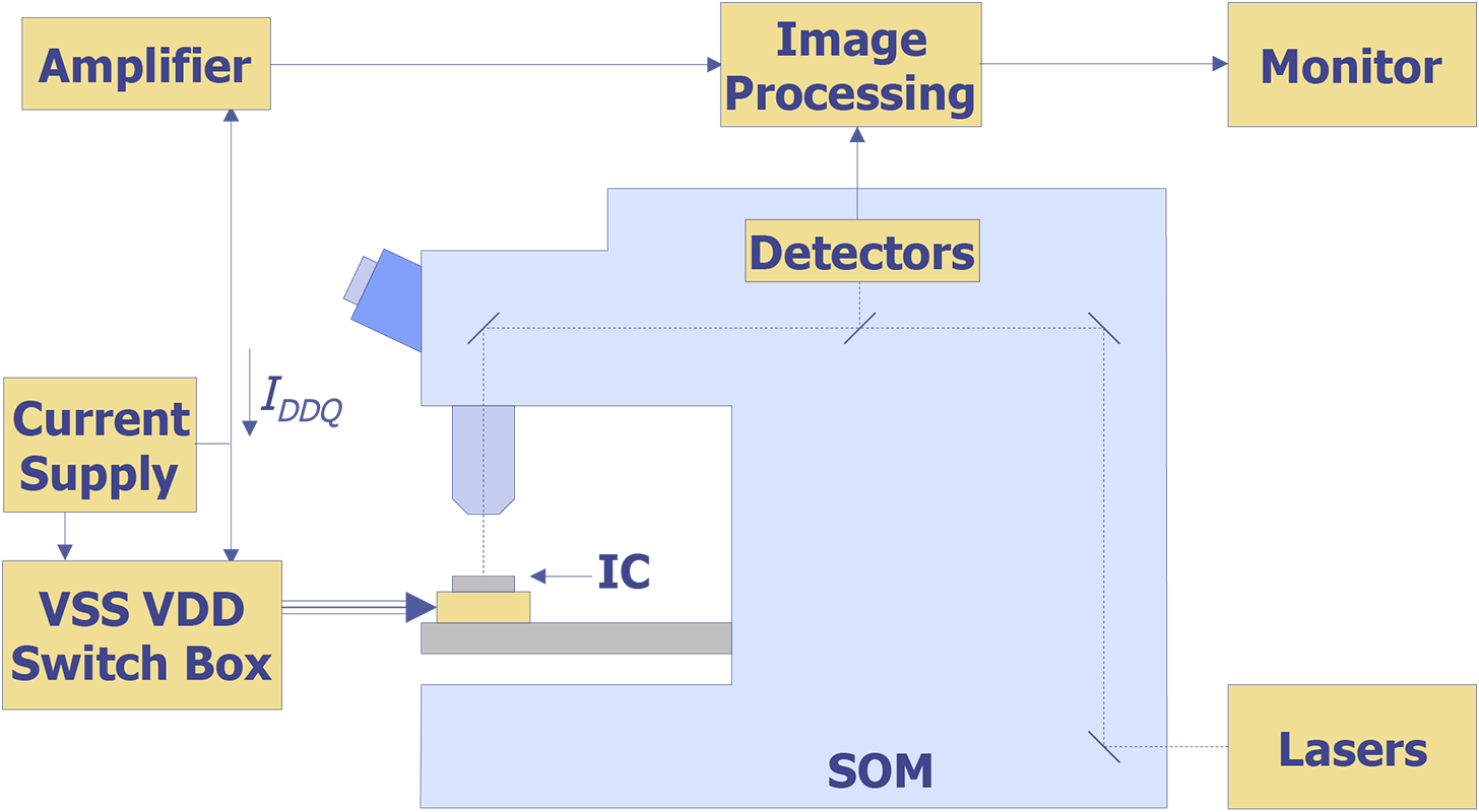
236 source measurement unit. This supply is used initially as a constant voltage supply at an appropriate voltage (typically within the IC's rated VDD range) to determine that the IC is powered-up properly and to measure the current needed for LIVA analysis. The supply is then switched to the constant current mode for LIVA analysis. Electrical stimulus for the inputs is selected using a simple switch box or can be provided through a computer-controlled matrix or digital tester.
With constant power supply current supplied to the IC, VDD varies as the laser beam scans across the IC active circuit regions. The variation of VDD is amplified by an Ithaco 1201 voltage amplifier operating in the ac coupled mode. The amplifier gain and bandpass filters (both high and low pass) are adjusted to optimize the specific LIVA image. The output of the amplifier is connected directly into the SOM's OBIC port.
LIVA, like OBIC, takes advantage of photon generated electron-hole pairs to yield information about IC defects and functionality. When electron-hole pairs are generated near the interface between differently doped regions in an unbiased IC, the charge carriers are separated by the built-in potential between areas with different Fermi levels. Biasing an IC can increase or decrease the Fermi level difference between regions, thereby altering the magnitude of electron-hole pair separation. LIVA images are produced by monitoring the voltage changes of the constant current power supply as the optical beam from the SOM is scanned across an IC. Voltage changes occur when the electron-hole pair recombination current increases or decreases the power demands of the IC.
The LIVA measurement and imaging of voltage shifts has two advantages beyond directly observing the photocurrents or IDDQ. First, the IC will act as its own current to voltage amplifier, producing a much larger LIVA voltage signal than photocurrent signal. This is in part due to the difference in "scale" for IC voltage and current. Figs. 2 and 3 illustrate this difference in "scale." Fig. 2 shows the I-V characteristics of a CMOS IC made with a p-well technology. The curves in Fig. 2 were generated by sweeping VDD from 10 to 0 V while the IC was biased in the static burn-in configuration. Individual transistor channels were illuminated by operating the SOM in spot mode and positioning the 633 nm laser in the middle of the polysilicon gate. The intensity of the 5 mW laser was reduced to 10% using one of the neutral density filters. As expected, the IC current increases when transistors are exposed to illumination.
Note that the increase in IDDQ with illumination is greater for "off" transistors than for "on" transistors. When a transistor is "off," there is a greater voltage between its source and drain than when the transistor is "on." This change in potential produces a difference in recombination current and in IDDQ. (It is this IDDQ difference has been used to identify logic states with photon exposure [2].)
Fig. 2 also shows that the IDDQ difference between the "off" and "on" states is greater for p-channel transistors than for n-channel transistors. This effect is explained by considering the recombination current for p-wells in n-substrates. Electron-hole pairs produced in the n-channel transistors will have recombination current across the p-well to n-substrate junction as well as source to drain current. The p-well to n-substrate current is independent of the IC logic state. Therefore, illuminating the n-channel transistors in different logic states has a smaller relative effect than illuminating the p-channel transistors in different logic states.


Fig. 3 is a V-I curve produced by sweeping the supply current from 250 to 0 nA. Fig. 3 data were generated by configuring and illuminating transistors in the same manner as in Fig. 2. While the curves in Figs. 2 and 3 have similar shape, the change in "scale" can be observed by examining the differences at a given bias point. For example, in Fig. 2 at 5 V the "off" p-channel transistor had a photocurrent increase of 80 nA (from 90 to 170 nA) when exposed to the SOM beam. The same transistor when supplied with 90 nA of current had a voltage decrease of 2.4 V (from 5 to 2.6 V) when exposed to the SOM beam. This large difference in signal, 2.4 V versus 80 nA, illustrates how the IC acts as its own current to voltage amplifier during LIVA analysis. Amplification would be required to make use of the 80 nA signal for imaging.


The second advantage of the LIVA approach versus direct photocurrent observation is that IC voltages are simpler to use than IC currents. While this may not appear to be too great an advantage at first, there are several important ramifications. Current measurement is done in series. Most current amplification systems will have maximum current capability (typically 250 mA) that restricts the operational range without modifications. There is also the added complication of sometimes needing to measure a relatively small photocurrent against a large dc background current. Voltage measurements are made in parallel, with none of the power limitations of current measurement. Small changes in voltage are easily measured using an ac coupled amplifier much less affected by background dc voltages. The simpler equipment setup and relatively larger signal make LIVA more attractive than conventional photocurrent methods.
The LIVA signal generation described in the previous section considers photon interactions on non-defective ICs. Under identical illumination conditions, localized defects on ICs can generate LIVA signals 3 to 4 orders of magnitude greater than other LIVA signals from non-defective ICs. This difference in LIVA signal depends upon the defect type, but two basic mechanisms are responsible for the increase. First, the defect, because of its location in the IC amplifies the effects of normal photocurrents by altering the power demand of circuit elements connected to the defect region. Second, the defect region itself is a site of enhanced recombination compared to non-defective areas. Two types of defects illustrating the differences between these mechanisms are described below.
For example, junctions connected to open conductors amplify normal photocurrent effects to produce a larger LIVA signal. Photon injection and subsequent electron-hole pair production will initially produce a normal LIVA signal at the defective junction. The recombination current generated will reduce the voltage across the junction. Normally, the transistor supplying the potential difference across the junction will quickly attempt to compensate for the recombination current and try to reestablish the initial bias conditions. If the interconnection path that supplies this "compensation charge" is open, then no compensation occurs and potential difference across the junction continues to decrease with photon injection. This can put the transistor directly associated with the open-circuited junction into saturation, increasing the IC's power demands. For constant current conditions, this results in a greater VDD decrease and a larger LIVA signal. Note also that the voltage of the open-circuited conductor connected to the junction will be the same as voltage of the junction. Therefore, any other transistor gates connected to the open conductor may also go into saturation, further amplifying the LIVA signal. When photon injection ceases, the junction voltage will slowly recover to its initial equilibrium voltage, which is determined by weak coupling of the open conductor to neighboring conductors, transistor bias, and parasitic leakage conditions [13].
If the open conductor has a significant amount of quantum mechanical tunneling (typical of stress void open conductors), the recovery to initial conditions will be much faster (on the order of milliseconds) [13]. However, large LIVA signals can still be generated because the electron-hole pair recombination current at the junction can be greater than the tunneling current.
Of course, if the IC logic state creates no potential difference across the open-circuited junction, there will be no LIVA signal.
Electrostatic discharge (ESD) damage of an input protection diode is an example of a defect that can cause a direct increase in recombination current. The changes in local Fermi levels caused by dopant redistribution and newly formed charge leakage paths will normally produce elevated IDDQ with no illumination. Electron-hole pair generation and recombination due to illumination in the area of the defect will produce even greater amounts of "leakage current." Holding the supply current constant will result in a decreased supply voltage and, consequently, an increased LIVA signal.
In both of the cases described above, the large increase in LIVA signals from defects facilitates rapid localization of the defective regions while scanning the entire IC die.
One final note about LIVA acquisition concerns the use of the ac coupled amplification system. As alluded to previously, one advantage of using ac coupled amplification is the mitigation of any dc offset signals that can complicate data acquisition. Another advantage is the use of an "over-supply" approach, which increases the effective bandwidth of the LIVA system for strong LIVA signals. Increased system bandwidth enables the analyst to acquire images faster without sacrificing spatial resolution.
The "over-supply" method involves increasing the supply current of the constant current source well above the maximum current needed to maintain the compliance voltage of the power supply. The compliance voltage (5 V for the examples in this paper) prevents damage to the IC from overvoltage. If the constant current supply had infinite bandwidth, no LIVA signal would be produced under "over-supply" conditions. Because the current source does have bandwidth (response time) limitations, supply voltage will momentarily decrease as the current source attempts to manage power demands. Amplifying the momentary voltage reductions produces the LIVA signal. The resultant system bandwidth is determined by the constant current source's bandwidth. We have used this "over-supply" LIVA approach for CIVA, enabling image acquisition of an entire IC die while the electron beam is scanned at TV rates.
The LIVA imaging approach described above can be used in two basic modes: defect localization and logic state determination. Examples of each are given below.
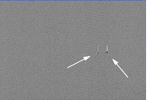
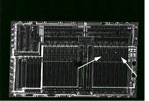
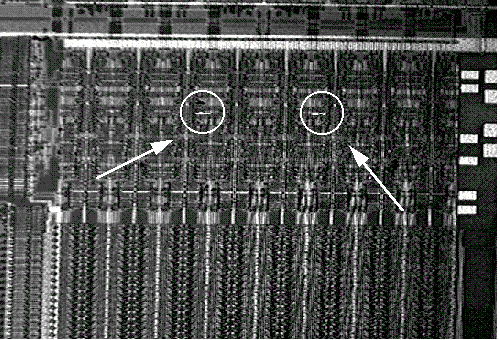
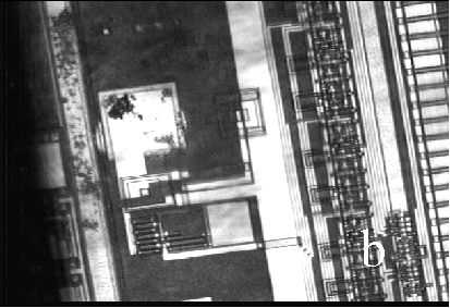
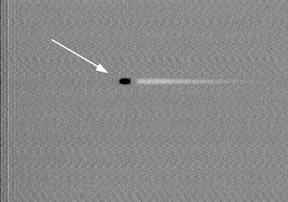
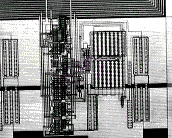
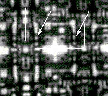
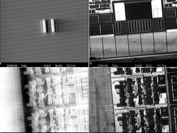
Localization of Open-Circuited Junctions: Figure 1 is a LIVA image of a passivated CMOS ASIC, the same type of IC used to produce the curves in Figs. 2 and 3. The 633 nm, 5 mW HeNe laser was used to acquire the LIVA images. The two small areas highlighted by arrows show the increased signal from two open-circuited junctions on the IC. The open-circuited junctions resulted from metallization stress voiding. The absence of any other signal in Figure 1 demonstrates the selectivity of LIVA for localizing defects. Figure 2 combines the LIVA image (white) and a reflected light image showing the same field of view as Figure 1. Figure 3 (see photographs) is a combined LIVA and reflected light image showing the two defects at increased magnification.
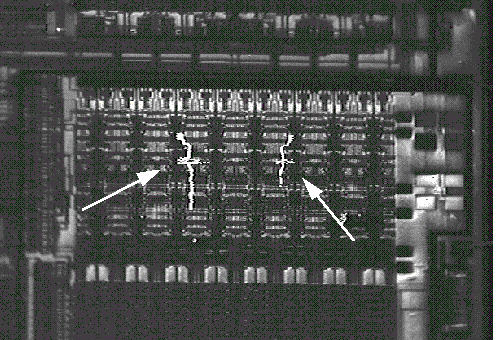
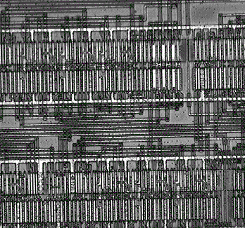
To confirm that the junctions seen in the LIVA image were indeed connected to open conductors, CIVA analysis was performed on the same IC. Figure 4 is a combined CIVA and secondary electron image that covers the approximate field of view shown in Fig. 3. Fig. 4 clearly shows the junctions directly associated with the open conductors in Fig. 3.
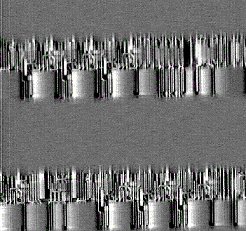
Figure 5 is a LIVA image illustrating the identification of transistor logic states. This image was acquired using the 633 nm HeNe laser used in Figs. 1-3. The IC is a CMOS microprocessor. The dark and bright areas indicate decreases and increases in the supply voltage, respectively. Bright contrast regions are produced as the SOM beam is masked from an "off" transistor by an opaque metal conductor, producing a return of the supply voltage to the non-illuminated condition. Note that the image is very similar in appearance to logic mapping with biased OBIC [1], but with the larger signal and ease of acquisition advantages of LIVA.
Figure 6 displays a LIVA difference image made from two images of the microprocessor in two different logic states. The field of view is the same as Fig. 5. The difference image was produced by a simple subtraction of two LIVA images, with the resultant image showing only those transistors that changed logic state. The metal interconnect between rows of logic cells does not produce a LIVA signal. The interconnect can be seen in Figure 7, a reflected light image at the same field of view as Figs. 6 and 7.
The LIVA defect localization and logic state detection demonstrated in the previous sections work well assuming photons can reach the junctions of interest. However, these techniques are impossible if any optically opaque layer prevents photon penetration. Flip-chip packaged ICs and ICs with multi-level metal interconnection would be very difficult to examine with LIVA using a visible light source. Infrared (IR) illumination for LIVA from a polished IC backside circumvents these problems. Backside examination of ICs has been well established and takes advantage of silicon's transparency to photons with energies less than the indirect silicon bandgap energy. Fig. 5 (see next page) displays the transmission coefficient of photons in (a) p- silicon and (b) p+ silicon as a function of wavelength [15]. The figure also shows wavelengths corresponding to the indirect bandgap energy in silicon and several laser wavelenths. Generation of LIVA signals from backside IR illumination is somewhat more difficult than reflected light IR microscopy because the photon wavelength must be long enough to penetrate through the silicon substrate, but short enough (have enough energy) to produce electron-hole pairs in the junction regions.


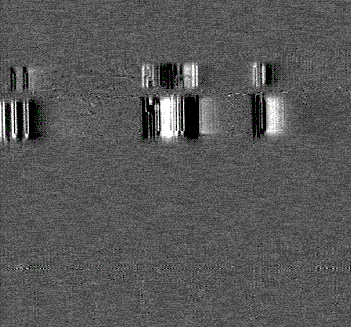
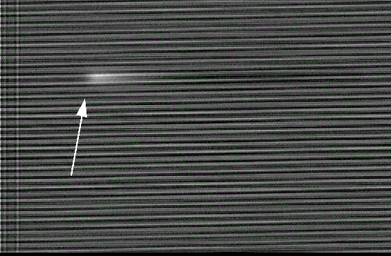
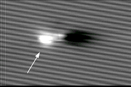
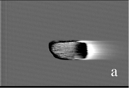
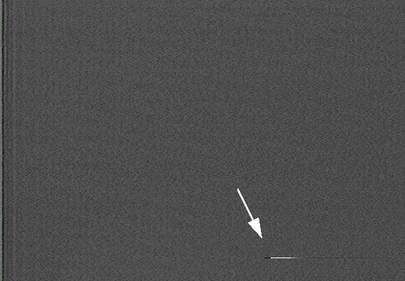
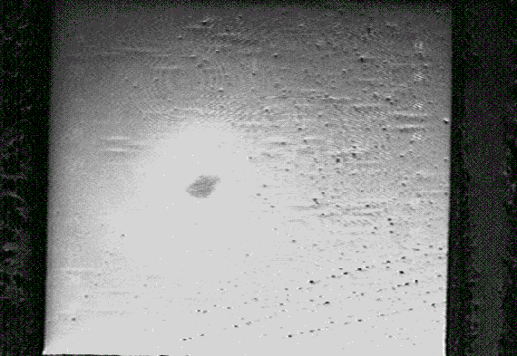
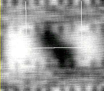
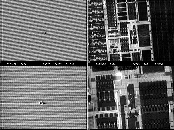
Backside IR Localization of Defects: Initial backside LIVA experiments were performed with the 1152 nm, 5 mW, HeNe laser. Figure 8 is a polished backside LIVA image of a 64K CMOS SRAM fabricated with a 2 micron, 2 level metal technology. The LIVA signal indicated by the arrow results from a floating input. The LIVA signal is much weaker than those shown in Fig. 1, as evidenced by the 60 cycle noise in Fig 8. The photon energy of the 1152 nm laser is just below the indirect silicon bandgap energy, but close enough for some electron-hole pair production (due to the energy level distribution). Figure 9 is a reflected IR micrograph of the same field of view as Fig. 8. The large depth of field of the low magnification objective used in Fig. 9 generates an image that has both the die frontside and backside in focus. This prevents IC frontside structures from being observed at low magnification. Figure 10 and Figure 11 are higher magnification IR LIVA and reflected IR images of the open SRAM input.
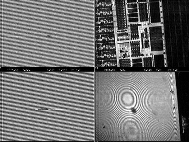
A stronger backside IR LIVA signal was produced from an SRAM input with ESD damage. Figure 12 and Figure 13 are IR LIVA and reflected IR images of an input with ESD damage. The LIVA signal is generated at the VDD input protection diode.
A radiation-hardened version of the Intel 80C51 fabricated at Sandia was also examined using IR LIVA. The microcontroller was fabricated using a 1.25 micron, 2 level metal, 2 level polysilicon technology. Earlier failure analysis using CIVA had identified open metal-1 to silicon contacts resulting from a pellicle scratch [16]. The contacts were completely obscured from surface optical examination by a metal-2 power bus.
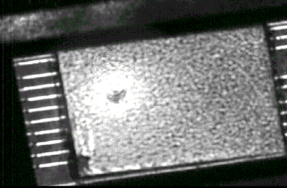
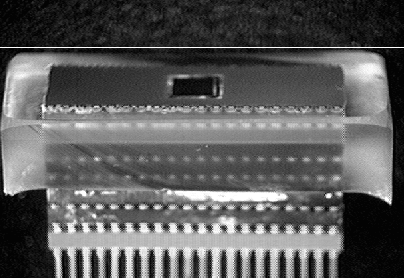
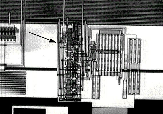
The microcontroller was packaged in a 40 pin ceramic dual in-line package (DIP). To gain access to the die backside the package was delidded and extensions (approximately 3") to the DIP's I/O pins were mounted on the top of the package. In order to hold the die in place during backside polishing, the entire assembly was potted in Epon 815 epoxy. Epon epoxy was chosen because of its low curing temperature (27oC) and negligible expansion [17]. The backside of the ceramic package was then polished until the die back was exposed. Figure 14 shows the package after polishing.
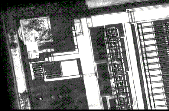
Figure 15 is a backside IR LIVA image of the entire microcontroller. The small LIVA signal indicated by the arrow is produced by the open metal-1 to silicon contact region. Figure 16 is a reflected IR image showing the same field of view as 15. Figure 17 and Figure 18 are backside IR LIVA and reflected IR images of the same defect site at higher magnification. The wide metal-2 bus obscuring frontside observation of the contacts can be seen in Fig. 18. Biased OBIC using 1010 gain and backside light emission were both attempted at the failure site identified with LIVA in Fig. 17. No anomalies were detected using either technique.
Backside IR Logic State Mapping: Even with the signal gain made possible by LIVA imaging, logic states could not be observed with the 1152 nm, 5 mW HeNe laser. The wavelengths of the two additional lasers used to attempt backside IR logic state mapping with LIVA are indicated in Fig. 5. Both are relatively inexpensive, water cooled Nd:YAG lasers. Initially, the1320 nm, 320 mW laser was used. Very high contrast reflected IR images were produced with the laser, but the photon energy was too low to produce electron-hole pairs. The defects observed earlier at 1152 nm were not visible in LIVA images using the1320 nm laser.
As shown in Fig. 5, the 1064 nm laser is attenuated significantly more than the other two IR lasers, but this wavelength was recently shown to be successful in backside OBIC imaging of thinned, heavily doped silicon [15]. It was hoped that the added power of the 1.2 W laser would compensate for the increase in silicon absorption.
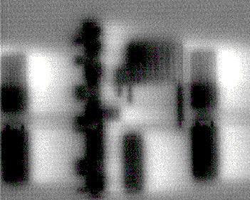
Figure 19 demonstrates that the 1064 nm, 1.2 W laser was indeed successful in producing backside IR logic state maps using LIVA. In fact, the signal strength was sufficient to view logic states with the laser power reduced by a factor of 10 with a neutral density filter. Fig. 19 shows an I/O structure from the microcontroller in a logical "1" state. The "off" transistors produce the dark contrast. As opposed to LIVA surface imaging, bright signals from metal do not obscure the LIVA signal from the transistor junctions. Figure 20 is a LIVA difference image showing the transistors that change state when the output of the I/O structure goes from a logical "1" to a logical "0". Figure 21 is a reflected IR image showing the same field of view as Figs. 19 and 20. The p-channel transistor highlighted by the arrow is described in the IR Optical Logic State Control section that follows.
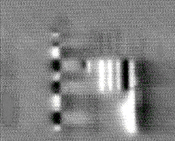
A second example of backside IR logic mapping using LIVA is shown in Figure 22, a LIVA image showing a portion of the SRAM on the microcontroller. No filters were used to attenuate the laser intensity. Each CMOS memory cell is composed of 6 transistors (4 transistors in the cross-coupled inverters and 2 n-channel access transistors). The dark areas are p-channel transistors in the "off" state. From this map one can easily determine the logic state of the SRAM memory cell. Figure 23 is a reflected IR image for registration.
In addition to performing defect localization and logic state determination, the photon probe can also change the logic state of a transistor. This effect of inducing enough photocurrent in a transistor to force the transistor "on" has been observed by several researchers [3,4]. Of course, if the transistor is driven by an internal source that can override the photon-induced preferred state, that source will determine the logic state. Optical logic state control can still be performed, but the choice of which transistors to illuminate becomes more complicated. Our success with backside IR LIVA indicated that we should be able to extend frontside logic state control using visible illumination into a tool for backside selection of logic states using IR illumination.
As a demonstration vehicle, optical logic state control using IR illumination was applied to the microcontroller SRAM shown in Fig. 22. Figure 24 shows a higher magnification image of a portion of an SRAM cell. The memory cell's two p-channel transistor gates are highlighted. Precise control of areas to be illuminated in the SOM is achieved by operating the SOM in spot mode and positioning the laser spot to the desired location. By illuminating only one p-channel transistor gate region in a SRAM cell, that transistor could repeatedly be turned "on" at IC power-up, effectively embedding that particular SRAM bit in the microcontroller.
Figure 19 illustrates a second example of backside IR optical logic state control. The arrow in Fig. 21 indicates the location of a p-channel transistor in a half latch circuit that holds the logic state of the I/O pin when tristated. By illuminating the active gate region of this transistor during power-up, the I/O structure was forced to a logical "1" state. Absence of illumination during the power-up state produced either a logical "1" or "0," with a preference for the "0" state. Clearly, these two examples indicate that optical logic state control can be used during backside analysis of ICs.
The three photon probing failure analysis methods described in this paper provide nondestructive, enhanced IC evaluation and failure localization capabilities for both front and backside IC examination. All three techniques are easily implemented on existing SOM equipment. They are powerful new additions to the set of IC analysis tools.
Standard Light Induced Voltage Alteration performed on the frontside of a standard packaged IC is not destructive and, like backside LIVA, can be performed simultaneously with light emission. Light Induced Voltage Alteration on a flip-chip IC can be performed once the backside of the IC is exposed. LIVA requires that electrical connections be maintained to the IC, so if the delidding process or process used to expose the backside of the IC severs the package interconnect, LIVA cannot be performed.