System Maintenance occurs every Friday.
System Maintenance occurs every Friday.
Resistive Contrast Imaging (RCI) is a scanning electron microscopy (SEM) imaging mode that generates a relative resistance map between two test nodes of an integrated circuit (IC) or microelectronic conductor test structure. RCI generates resistance information by using the IC or test structure as a current divider. Because the IC is not biased, RCI does not require vectoring information. However, additional testing information can be very useful to effectively apply RCI.
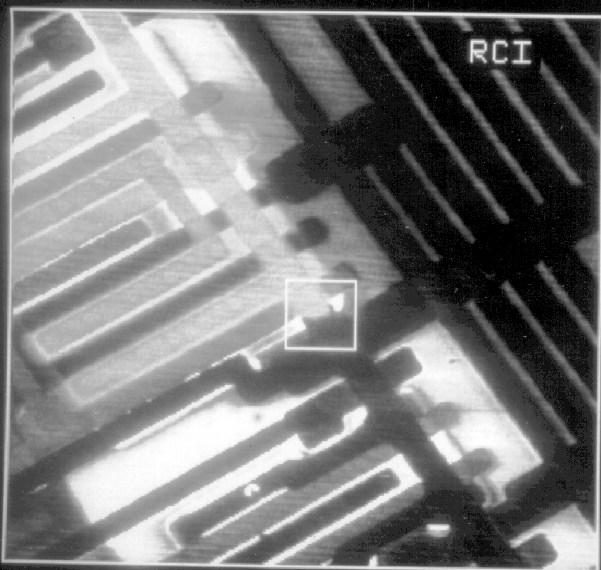
Defects in a resistive contrast image exhibit abrupt transitions from bright to dark because the resistance ratio is different on one side of the defect as opposed to the other side. The following photograph illustrates an abrupt change in resistance in a VDD line on a standard cell design.
Figure 1 - Resistive Contrast Image of Open VDD line.
The open VDD line in the figure displays how RCI can be used effectively on ICs. The open conductor has a direct resistance path to the power/ground test nodes typically used for RCI, the passivation is intact, the IC is not biased for RCI image collection, and the fine structure of this electromigration-produced open is clearly seen in the image. This area was identified for RCI analysis after light emission examination indicated a change in transistor saturation in this area.
While an abrupt change in contrast in the RCI image indicates a resistance change, independent confirmation of a failure site using capacitive-coupled voltage contrast (CCVC) is highly desirable. If both techniques indicate an open conductor site, then the failure has independent confirmation and a high probability of being an actual failure. If the two techniques disagree, then the reason for this disagreement must be resolved. Two possible reasons for disagreement are: 1) an open conductor with a large amount of quantum mechanical tunneling was detected in RCI but not in CCVC because the vectoring speed was too slow, or 2) an open conductor "seen" in the RCI image when an excessive primary electron beam energy is used. The excessive beam energy can change transistor threshold voltages and the unbiased off/on status of the transistors. This change in threshold voltage can change the resistive path of a conductor relative to the test nodes during the RCI image acquisition, producing a "false" RCI artifact open not seen in the CCVC image. Independent confirmation of an open using CCVC and RCI greatly reduces the chances of identifying an image artifact as the cause of failure.
Any open conductor site identified by RCI that was initially indicated by a light emission signature should be checked to verify that the open conductor produces the light emission. Open conductors usually are associated with light emission from transistors in saturation; therefore, the conductor identified with RCI should be connected to the light emitting transistors. This "connection" can be indirect. For example, the open conductor may directly put p-channel transistors into saturation, which then drives associated n-channel transistors into saturation. Since light emission is approximately 3 orders of magnitude greater for n-channel transistors than p-channel transistors, only the n-channel transistors may be visible in the light emission images.
This verification is necessary to ensure that the open conductor identified by RCI is the cause of light emission. If not, then another failure mechanism may be occurring independent of the open conductor.
Since RCI requires interaction between the primary electron beam and the conductors of interest, passivation and optically opaque layers may be "probed through" by increasing the primary electron beam energy. The following expression can be used for a rough estimate of the primary beam energy required to reach a given conductor:
R=0.022 E1.65
where R is the distance below the surface and E is the primary electron beam energy.
Because RCI "images" a fraction of the primary electron beam current, the more the primary electron beam current increases, the more the RCI signal increases. Normally, an amplifier gain of 109 is required for RCI imaging. If no RCI signal is present at 5kV, decrease the beam current, increase the beam energy, and increase the beam current once again until an RCI signal appears. Repeat this increasing beam energy sequence until the top level of conductors appears in the RCI image. Lower levels of conductors will require higher beam energies to be reached/imaged.
RCI is performed if an open conductor is suspected on an IC or conductor test structure. Shorts can be detected, but only the fact that two conductors are shorted is revealed. The location of the short does not produce RCI contrast.
The RCI technique is the preferred method for examining test structures-- such as thin film resistor chains, metal serpentines, or IC structures--that do not involve transistors.
For an IC, the RCI technique can be effective in localizing an open conductor, but three limitations reduce the technique's effectiveness. First, only resistance differences relative to the test nodes are identified in RCI. For example, a large resistance difference in a complicated feedback network will not be identified if there is no resistance difference relative to the device leads. Second, another induced current effect, electron beam induced current (EBIC), should be avoided. EBIC generates currents several orders of magnitude greater that RCI and can mask the RCI signals. EBIC signals are generated primarily from buried diffusions and can be avoided by using lower primary electron beam energies. (On MOS structures, the EBIC signal also indicates a primary electron beam energy sufficient to reach the gate oxide structures and produce irradiation damage. Lower primary beam energies reduce/eliminate the irradiation effects.) Unfortunately, most SEMs do not have continuous electron beam energy selection. The primary beam energy sufficient for RCI may include some EBIC signal, but the next lower primary beam energy available is too low for any RCI (or EBIC) signal. Third, even if there are no access or EBIC limitations, the RCI signal will normally include resistance information from most of the conductors on the IC using power and ground as test nodes. This will make it difficult to identify the site of an open conductor because of all the additional information in the image. Using light emission, liquid crystals, or another failure analysis technique to reduce the area for RCI examination will reduce the amount of extra RCI information and increase the likelihood of locating an open conductor.
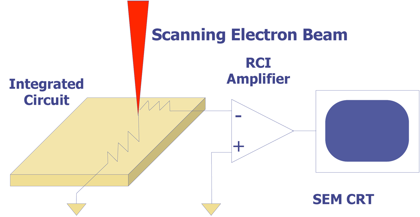
To obtain RCI information, the primary electron beam energy is increased until the tip of the interaction volume intersects the buried conductors of interest. Under these conditions, a portion of the primary electron beam current will be injected into the conductor. Using an amplification configuration as shown in Figure 2, the currents injected by the primary electron beam will have a path out of the IC or test structure. The relative resistance between the electron beam position on the sample and the test nodes will determine the direction and amplitude of current flow. The current, approximately 1 nA or less, is amplified and used to make a resistance map of the conductors. Using higher primary beam currents will increase the RCI signal. Usually, the power and ground inputs are used as test nodes because of their global nature across the IC; however, other node combinations may be used if indicated by the failure history. For conductor test structures, such as metal serpentines, the two ends of the test structure should be used as the test nodes.
Since RCI requires interaction between the primary electron beam and the conductors of interest, optically opaque layers may be "probed through" by increasing the primary electron beam energy. The following expression can be used for a rough estimate of the primary beam energy required to reach a given conductor:
R=0.022 E1.65
where R is the distance below the surface and E is the primary electron beam energy.
Because no irradiation damage occurs in test structures with no gate oxide or oxide capacitors, starting with a very high primary electron beam energy is possible. This will ensure that the primary electron interaction volume reaches the buried conductor and reduce surface passivation charging by "shorting" the substrate to the surface through the interaction volume.
For ICs, RCI should be performed after other, more benign failure analysis techniques have been applied. Even though RCI can be used in a "non-destructive" fashion (causing very little irradiation damage to the oxide gates of an MOS IC), the possibility of altering IC operation with primary electron beam energies greater than 1.0 kV still exists. RCI does have the advantage of being able to probe through passivation and metal layers. If an open conductor is indicated by other test methods, RCI should be applied before layer removal. If the IC can be biased and open conductors are indicated, the charge-induced voltage alteration (CIVA) technique is preferred over RCI because of its higher selectivity and sensitivity. IC structures without transistors, such at thin-film resistance networks, are not suitable to CIVA and RCI is the preferred method for this type of structure.
For IC test structures such as electromigration serpentines, RCI should be applied after an open conductor or large increase in resistance is indicated. No MOS structure is in place to be altered by primary beam irradiation, so high energies can be used to ensure that the interaction volume reaches the structures of interest. The higher energies will also reduce surface charging by "shorting" the surface passivation to the substrate. While surface layer removal can make it easier to reach a buried conductor pattern at lower primary electron beam energies, care must be taken not to alter the failing conductor state during deprocessing. RCI can eliminate or reduce the need for surface layer removal during failure site localization.