System Maintenance occurs every Friday.

Scanning Electron Microscope

Are you looking for more information regarding this and other subjects? Look no further than Semitracks' Online Training. Semitracks' Online Training contains short courses and other material useful for any Engineer trying to learn new subjects or brush up on old ones.

What is an SEM Examination?

History

In 1938, von Ardenne added scan coils to a transmission electron microscope (TEM), producing a scanning transmission electron microscope (STEM). In 1942, Zworykin and his team developed the first scanning electron microscope to employ secondary electron detection. He and his team recognized that secondary electron emission could be used to generate an image showing the topographic contrast of a specimen. The collector was biased to +50 volts to capture the secondary electrons, and the voltage drop across a connected resistor generated the image. Although the initial spatial resolutions were poor, approximately 200 nm, Zworykin and his colleagues reduced the beam spot size and obtained images with a resolution of 50 nm. In the late 1940s and early 1950s, researchers Oatley and McMullin introduced several notable improvements to the scanning electron microscope, including the electromagnetic lens, the stigmator, and signal amplification. By attaching the scintillator directly to the face of the photomultiplier, Everhart and Thornley greatly improved the signal-to-noise ratios.

The two most notable developments to the scanning electron microscope in the 1960s were the development of the LaB6 (Lanthanum-hexaboride) electron cathode and the revival of the field emission tip electron source. The LaB6 improves resolution via a high-brightness electron gun. Yielding even higher resolution, the field emission tip electron source produces current densities that measure thousands of amps per cm2. Consequently, today's commercial SEMs can obtain resolutions of about 10-20Å. In 1968, Fitzgerald demonstrated the addition of an energy-dispersive x-ray detector to an SEM, moving the SEM into the analytical probe arena.

SEM Basics

Electron Optics

Three types of electron guns are used on today's scanning electron microscopes: 1. the tungsten cathode, 2. the lanthanum hexaboride (LaB6) cathode, and the field emission gun. The three electron guns are described briefly below.

Tungsten cathode

The tungsten cathode is a fine wire approximately 100mm in diameter that has been bent into the shape of a hairpin with a V-shaped tip. The tip is heated by passing current through it; normally, the tip is heated to around 2400°C. At this temperature, an appropriate current density measures approximately 1.75 A/cm2. The electrons will have a potential distribution of 0 to 2 volts. With a bias voltage between 0 and 500 volts, the electrons can be accelerated toward the anode. At an emission of 1.75 A/cm2, the tungsten filament lasts approximately 50 hours. A schematic diagram of a tungsten cathode is shown below (see Figure 1).

Schematic of a tungsten filament (self-biased) electron gun (after Goldstein et. al.). Schematic of a tungsten filament (self-biased) electron gun (after Goldstein et. al.).
Schematic of a tungsten filament (self-biased) electron gun (after Goldstein et. al.).

Lanthanum hexaboride (LaB6) cathode

As the need for higher resolution imaging increased, so did the need for brighter filaments. The most straightforward method to achieve this goal is to find a material with a lower work function Ew. A lower work function means more electrons at a given temperature, hence a brighter filament and higher resolution. Lanthanum hexaboride, commonly known as LaB6, has been the best material developed to date for this application. The LaB6 filament operates at approximately 2125°C and is five times brighter than a tungsten filament under the same conditions. However, LaB6 filaments tend to be more expensive than tungsten filaments. A schematic of the LaB6 filament is shown in Figure 2.

Gun configuration for a LaB6 cathode (after Goldstein et. al.). Gun configuration for a LaB6 cathode (after Goldstein et. al.).
Gun configuration for a LaB6 cathode (after Goldstein et. al.).

Field Emission Gun

Another method for generating electrons is the field emission gun. When the cathode forms a very sharp tip (typically 100 nm or less) and the cathode is placed at a negative potential with respect to the anode so that the local field at the tip is very strong (greater than 107 V/cm), electrons can tunnel through the potential barrier and become free. Although the total current is lower than either the tungsten or the LaB6 emitters, the current density is between 103 and 106 A/cm. Thus, the field emission gun is hundreds of times brighter than a thermionic emission source. Furthermore, since the electrons are field generated rather than thermally generated, the tip remains at room temperature.

Tips are usually made from tungsten etched in the <111> plane to generate the lowest work function. Because a native oxide will quickly form on the tip even at moderate vacuum levels (10 µPa), a high vacuum system (10 nPa) is needed. To keep the tip diameter sufficiently small, the cathode warmed to 800-1000 °C or rapidly heated to approximately 2000 °C for a few seconds to blow off material. A schematic of a field emission tip is shown in Figure 3.

Gun configuration for field emission (after Goldstein et. al.). Gun configuration for field emission (after Goldstein et. al.).
Gun configuration for field emission (after Goldstein et. al.).

Electron Lenses

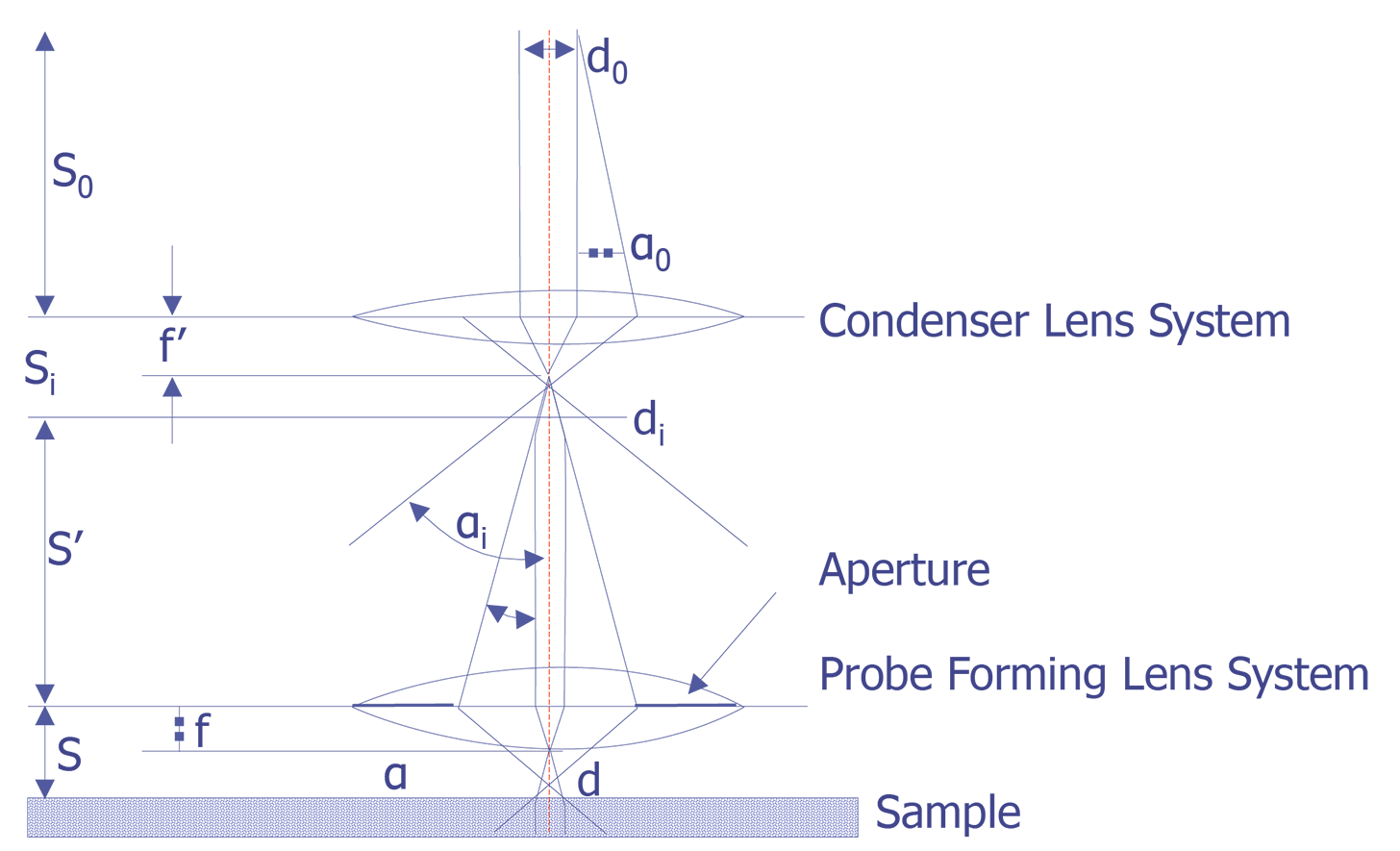
The electron beam is focused using electromagnetic lenses. The condenser lens system, which is composed of one or more lenses, determines the beam current that impinges on the sample. The probe-forming lens, often called the objective lens, determines the final spot size of the electron beam. Conventional electromagnetic lenses are used, and the interaction of the electromagnetic field of the lens on the moving electrons focuses the electron beam.

Figure 4 depicts the scanning electron microscope column. The a angles drawn in Figure 4 are exaggerated on purpose to more clearly show the effect of the lenses on the electron optics. Depending on the working distance, the probe lens can be adjusted to focus the beam. The working distance is defined as the distance between the bottom pole piece of the objective lens and the sample surface. It typically measures 5 to 25 mm. As the working distance is increased, the spot size increases on the sample, given the same final aperture lens.

There is a second tradeoff between spot size and beam current. The spot size is directly controlled by minimizing di (see Figure 4). However, by minimizing di, the beam current falls off by the ratio (aa/ai)2. The operator must decide whether the analysis requires minimizing the beam spot size or maximizing the beam current.

Schematic of ray traces in a typical scanning electron microscope column (after Goldstein et. al.). Schematic of ray traces in a typical scanning electron microscope column (after Goldstein et. al.).
Schematic of ray traces in a typical scanning electron microscope column (after Goldstein et. al.).

Several aberrations occur in an electron optical column, including spherical aberration, chromatic aberration, diffraction, and astigmatism. The first three are depicted schematically in Figure 5. Spherical aberration results from nonuniformity of the lenses. Electrons which pass through the lens further off the optical axis are pulled more strongly than those that pass through near the center of the lens. To reduce this effect, the final aperture can be reduced, but this reduction results in a lower beam current. Chromatic aberration results from differences in electron velocity through the lenses. The magnetic lenses will bend electrons with higher velocity or energy more strongly, resulting in a dull or blurred image. No method exists to correct this problem other than using a more expensive LaB6 or field emission instrument. Tungsten filament systems typically have a 2 eV spread when leaving the cathode; LaB6 systems have a 1 eV spread, and field emission systems have a 0.2 to 0.5 eV spread. Diffraction occurs because of the wave nature of electrons and the aperture size of the final lens. The only way to reduce diffraction problems is to increase the final aperture size.

Astigmatism results from the fact that magnetic lenses do not have perfect symmetry. Machining errors can cause lens systems to be slightly elliptical rather than perfectly circular, and irregularities in the iron windings can cause variations in the magnetic field. Most instruments contain a stigmator in the final lens system to help compensate for this effect. The stigmator usually has two controls, one to correct for the magnitude of the asymmetry and one to correct for the direction of the asymmetry of the main field. The stigmator can only correct asymmetry in the final lens; it cannot correct dirty aperture or filament misalignment.

Schematic drawings showing spherical and chromatic aberrations, as well as diffraction at a lens aperture (adapted from Hall, Oatley, and Goldstein et. al.). Schematic drawings showing spherical and chromatic aberrations, as well as diffraction at a lens aperture (adapted from Hall, Oatley, and Goldstein et. al.).
Schematic drawings showing spherical and chromatic aberrations, as well as diffraction at a lens aperture (adapted from Hall, Oatley, and Goldstein et. al.).

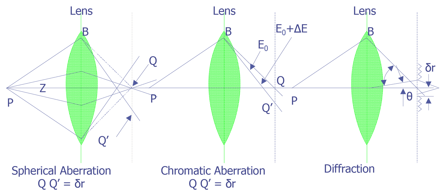
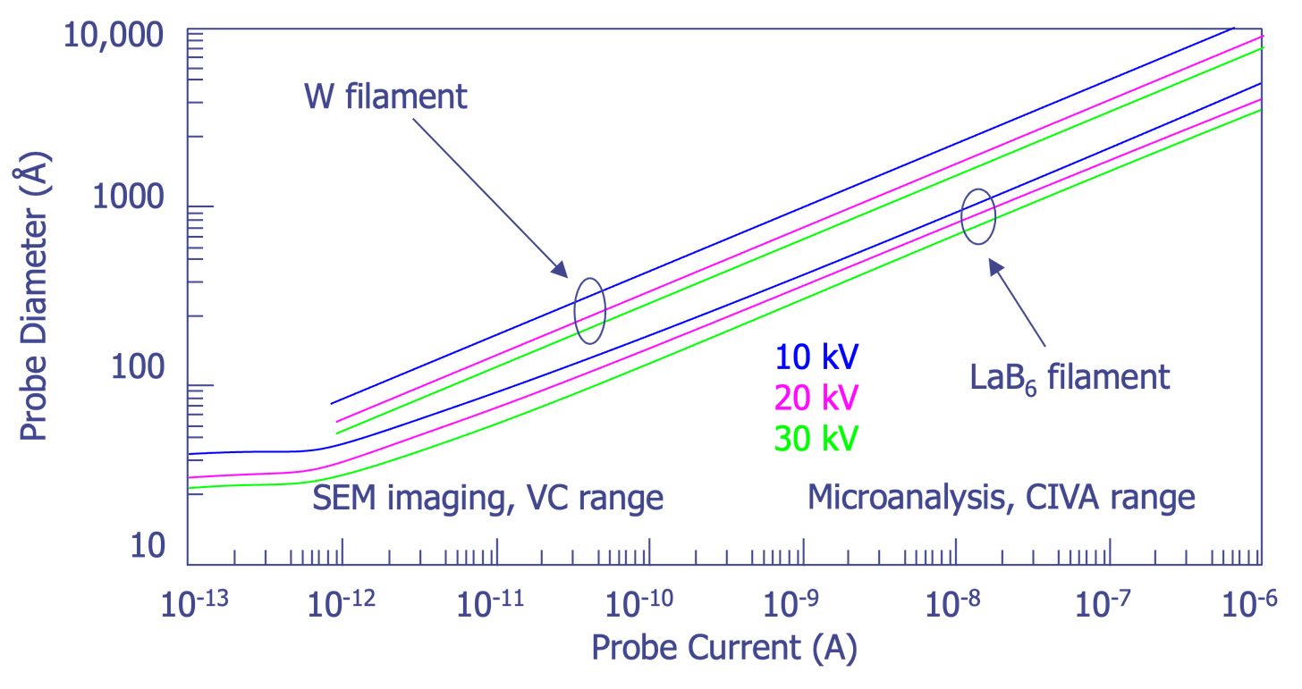
Figure 6 shows the relationship between probe current and beam diameter for both tungsten and LaB6 systems. These values were taken with the tungsten gun current density at 4.1 A/cm2 and the LaB6 gun current density at 25 A/cm2.

Relationship between probe current and the size of the electron beam. Calculations use the W hairpin filament and the LaB6 gun operating at 15 and 30 kV (after Goldstein et. al.). Relationship between probe current and the size of the electron beam. Calculations use the W hairpin filament and the LaB6 gun operating at 15 and 30 kV (after Goldstein et. al.).
Relationship between probe current and the size of the electron beam. Calculations use the W hairpin filament and the LaB6 gun operating at 15 and 30 kV (after Goldstein et. al.).

Electron Beam/Specimen Interactions

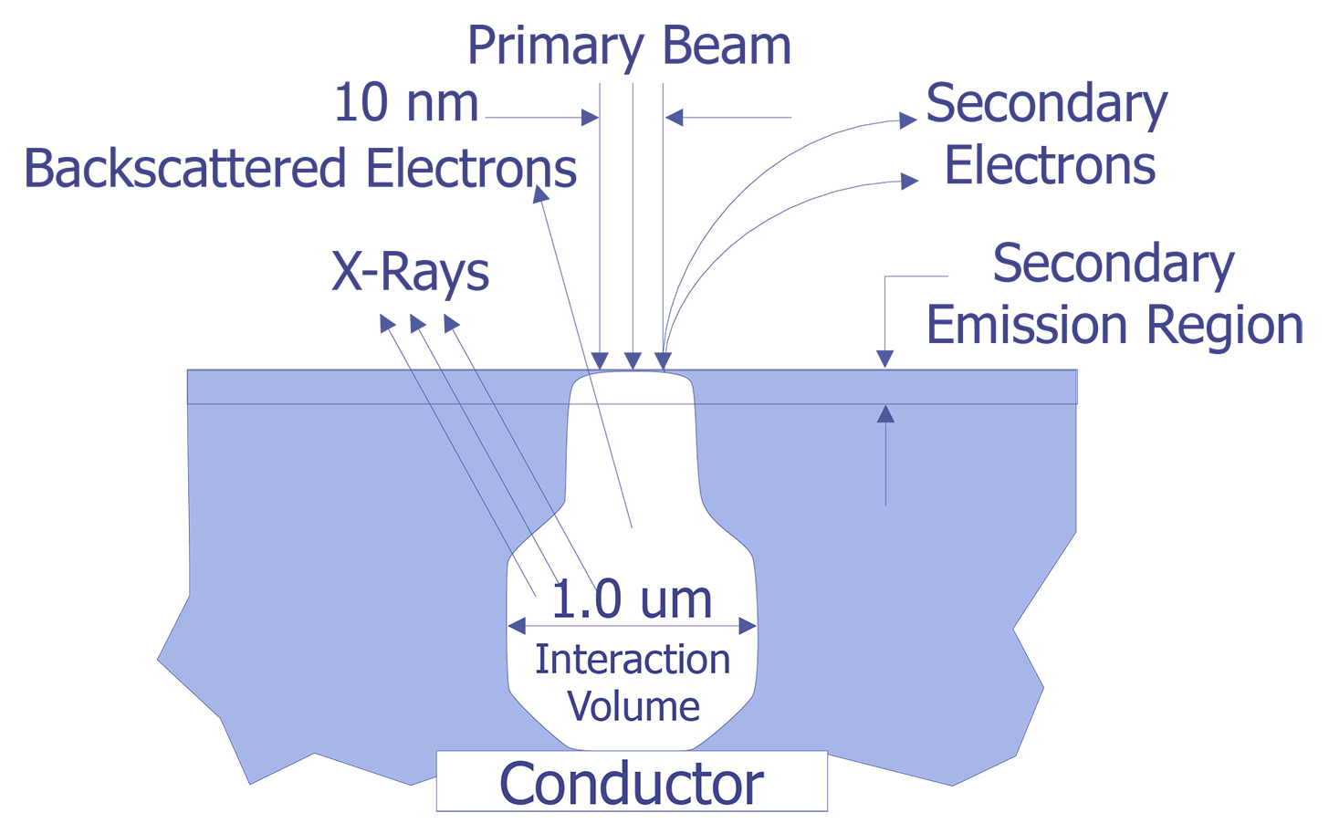
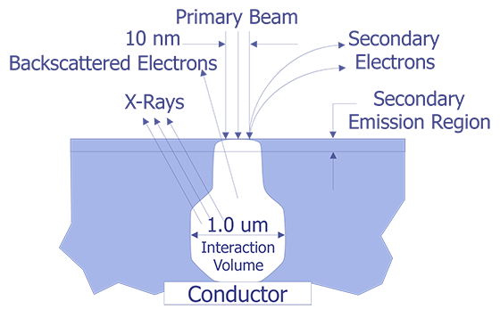
Electron beam interactions can be divided into two categories: elastic interactions and inelastic interactions. Elastic scattering occurs when the energy of the scattered electron is the same as the energy of the incident electron, i.e., no energy is transferred from the beam into the specimen. Elastic scattering causes the beam to diffuse through the sample. Inelastic scattering results when the incident electron loses energy in its interaction with the sample. A number of different processes (including plasmon excitation, excitation of conduction electrons leading to secondary electron emission, ionization of inner shells, Bremsstrahlung or Continuum x-Rays, and excitation of phonons) can cause inelastic scattering-- in other words, the slowing of electrons as they penetrate into the sample.

From these two phenomena originates the interaction volume (see Figure 7). The interaction volume, a teardrop shape, can be experimentally produced by spotting the electron beam in polymethylmethacrylate. The interaction volume can also be predicted by using Monte Carlo simulation. The shape of the interaction volume is dependent on three main parameters: the atomic number or density of the material, the beam energy, and the tilt angle. Monte Carlo simulation data indicate that the linear dimensions of the interaction volume tend to decrease with increasing atomic number or density when the accelerating voltage is kept fixed. Because the effect cross section for inelastic scattering increases, the electrons slow more rapidly, preventing them from significant lateral travel. The size of the interaction volume is a strong function of the beam energy because the effective cross section decreases as a square of the energy, Q ~ 1/E2. The effect of tilt on the interaction volume can be mainly attributed to forward scattering. As the sample is tilted more off axis, more forward scattering takes place, reducing the depth of the interaction volume. The range of the interaction volume, or rather its statistical depth, has been reduced to equation format by several researchers. The most common is the Kanaya-Okayama range, which is given below.

The Kanaya-Okayama range. The Kanaya-Okayama range.

where RKO is expressed in µm, E0 is given in keV, A in g/mol, ? in g/cm3, and Z is the atomic number of the target.

Electron Beam Physics Interaction Volume (after Cole). Electron Beam Physics Interaction Volume (after Cole).
Electron Beam Physics Interaction Volume (after Cole).

Backscattered Electrons

Approximately 30% of the incident electrons escape the sample by scattering. These electrons are known as backscattered electrons, and they provide a useful signal for SEM imaging. The fraction of backscattered electrons emitted from a sample depends on the atomic number of the elements in the sample. A sample with a high atomic number emits a greater fraction of backscattered electrons than a sample with a low atomic number. The backscatter coefficient e is defined as follows:

The backscatter coefficient e is defined by this equation. The backscatter coefficient e is defined by this equation.

where nBS is the number of backscattered electrons and nB is the number of beam electrons incident on the target. While the ratio of backscattered electrons depends on the atomic number of the sample, the ratio is almost independent of beam energy (see Figure 8). The ratio of backscattered electrons to incident electrons is also dependent on tilt angle; as the tilt angle increases, the ratio of backscattered electrons also increases.

Variation of the backscatter coefficient as a function of atomic number at E0 = 10 keV (blue) and E0 = 49 keV (red) (after Heinrich). Variation of the backscatter coefficient as a function of atomic number at E0 = 10 keV (blue) and E0 = 49 keV (red) (after Heinrich).
Variation of the backscatter coefficient as a function of atomic number at E0 = 10 keV (blue) and E0 = 49 keV (red) (after Heinrich).

Signals from Inelastic Scattering

Four signals result from inelastic scattering: (1) secondary electrons, (2) characteristic x-rays, (3) bremsstrahlung or continuum x-rays, and (4) cathodoluminescense radiation.

Secondary electrons comprise the electrons in region III shown in Figure 9. The upper portion of the distribution, region I, is the broad hump of electrons which have lost less than 40% of their incident energy due to inelastic scattering. A smaller fraction of beam electrons lose greater than 40% before escape the specimen, forming region II. The increase in electrons which forms region III is due to the process of secondary electron emission. Secondary electrons are emitted electrons that have an energy of less than 50 eV. Secondary electrons come from the top 1 to 10 nm of material in the sample, with metals characteristically exhibiting 1nm, and insulators characteristically exhibiting 10 nm. The secondary electron coefficient tends to be insensitive to atomic number; however, the coefficient depends on beam energy, as shown in Figure 10. Starting at zero energy, the secondary electron coefficient rises with increasing energy, reaching unity around 1 keV. The curve peaks at just over 1 for metals and as high as 5 for insulators, and then falls below unity between 2 and 3 keV. This region above unity tends to be a good beam energy for performing voltage contrast.

(a) Energy distribution of electrons emitted from a target over the entire energy range including backscattered electrons (regions I and II) and secondary electrons (region III). (b) Energy distribution both measured (blue) and as calculated (magenta) (after Goldstein et. al.). (a) Energy distribution of electrons emitted from a target over the entire energy range including backscattered electrons (regions I and II) and secondary electrons (region III). (b) Energy distribution both measured (blue) and as calculated (magenta) (after Goldstein et. al.).
(a) Energy distribution of electrons emitted from a target over the entire energy range including backscattered electrons (regions I and II) and secondary electrons (region III). (b) Energy distribution both measured (blue) and as calculated (magenta) (after Goldstein et. al.).
Schematic illustration of the total emitted electron coefficient (eta + delta) as a function of beam energy (after Goldstein et. al.). Schematic illustration of the total emitted electron coefficient (eta + delta) as a function of beam energy (after Goldstein et. al.).
Schematic illustration of the total emitted electron coefficient (η+δ) as a function of beam energy (after Goldstein et. al.).

X-rays can be generated by two different mechanisms. One is the interaction of the electron with the coulombic field of the atom core. This is the bremsstrahlung ("braking radiation") or x-ray continuum. The other mechanism is the interaction of the electron with an inner shell electron that results in an ejection of the inner shell electron. During the subsequent deexcitation, an outer shell electron will fall into the vacancy, releasing an x-ray.

Another product from inelastic scattering is the Auger electron. The Auger electron has an energy typical of the atom because the electron transitions occur between sharply defined energy levels. While characteristic x-rays have a longer mean free path, Auger electrons typically have a very short mean free path (approximately 0.1 - 2 nm) because Auger electrons have a fairly low energy range (50 eV to 2 keV).

Cathodoluminescence occurs when certain materials are bombarded with energetic electrons and emit long-wavelength photons in the ultraviolet and visible regions of the em spectrum. This effect only occurs in materials that have a full valence band, an empty conduction band, and a non-zero bandgap. When an energetic beam electron scatters inelastically in such a solid, electrons from the filled valence band can be promoted to the conduction band, leaving "holes." At some later point, if there is no external bias, the electron and hole will recombine and produce a photon.

Image Formation

As the electron beam strikes the sample surface, it produces detectable signals ranging from backscattered electrons, secondary electrons, absorbed electrons, characteristic and continuum x-rays, and cathodoluminescent radiation. By measuring these signals with suitable detectors, the analyst can gain information regarding the topography and composition at a single location. In order to study more than one single point, the beam must be scanned. Scanning is accomplished by driving electromagnetic coils arranged in sets consisting of two pairs, one pair each for deflection in the X and Y directions. A typical system, shown in Figure 11, has two sets of scan coils located in the final aperture.

Schematic illustration of scanning system of the scanning electron microscope. Abbreviations: FA, final aperature; SD, solid state electron detector; ET, Everhart-Thornley detector; S, scintillator; PM, photomultiplier; W, wavelength-dispersive x-ray spectrometer; ED, energy dispersive x-ray spectrometer; CRT, cathode ray tube (after Goldstein et. al.). Schematic illustration of scanning system of the scanning electron microscope. Abbreviations: FA, final aperature; SD, solid state electron detector; ET, Everhart-Thornley detector; S, scintillator; PM, photomultiplier; W, wavelength-dispersive x-ray spectrometer; ED, energy dispersive x-ray spectrometer; CRT, cathode ray tube (after Goldstein et. al.).
Schematic illustration of scanning system of the scanning electron microscope. Abbreviations: FA, final aperature; SD, solid state electron detector; ET, Everhart-Thornley detector; S, scintillator; PM, photomultiplier; W, wavelength-dispersive x-ray spectrometer; ED, energy dispersive x-ray spectrometer; CRT, cathode ray tube (after Goldstein et. al.).

The SEM image is constructed by creating a map of intensities from the detector of interest with respect to the x-y location of the electron beam. The information forms the basis for two principal types of displays: a line scan and an area scan. A line scan is generally formed by allowing the x position on the CRT to correspond to the x scan of the electron beam and using the y position on the CRT to display signal intensity. An area scan is generally formed by allowing the x and y position on the CRT to correspond to the x and y position of the scanned electron beam. The intensity of the beam is represented by the intensity of the signal on the CRT, sometimes referred to as "Z modulation."

Magnification in the SEM image is accomplished by adjusting the scale of the map on the CRT. Because the size of the CRT screen is fixed, magnification increases when the length of the scanned area decreases. Magnification depends on the excitation of the scan coils, not on the objective lens. Finally, the image does not rotate as the magnification is increased. The image rotates when the working distance is changed (the distance between the sample surface and the pole piece).

Another concept in SEM imaging is picture point versus picture element. Picture point is the region that constitutes a single spot on the CRT. On a digital SEM, the picture point would be the size of a single pixel. The picture element is the region on the sample surface where the beam interacts. For example, if the beam diameter is 50 nm and the resultant interaction volume for the secondary image is 100 nm, then the picture element is 100 nm. The minimum picture element is related to magnification by the following equation:

The minimum picture element is related to magnification by this equation. The minimum picture element is related to magnification by this equation.

This property creates hollow magnification. The magnification on the SEM can be set higher than the picture element diameter, leading to a fuzzy image.

Depth of field expresses the range of depth that an image appears to be in focus. Depth of field, D, can be determined by the equation D = 2r/a, where r is the maximum tolerable radius of the beam and a is the beam divergence. The beam divergence a can be expressed as a function of final aperture radius R and working distance D, where a = R/WD. Table 1 lists several combinations of magnification and aperture sizes and their resulting working distances.

Depth of Field at 10-mm Working Distance

Depth of field at 10 mm working distance.
Magnification 100-µm aperture (a = 5 x 10⁻³ rad) 200-µm aperture (a = 10-2 rad) 600-µm aperture (a = 3 x 10⁻² rad)
10 x 4 mm 2 mm 670 µm
50 x 800 µm 400 µm 133 µm
100 x 400 µm 200 µm 67 µm
500 x 80 µm 40 µm 13 µm
1000 x 40 µm 20 µm 6.7 µm
10,000 x 4 µm 2 µm 0.67 µm
100,000 x 0.4 µm 0.2 µm 67 nm

Detectors

Two types of detectors, electron detectors and cathodoluminescent detectors, are used in conjunction with the SEM. In failure analysis applications, electron detectors are of the most interest. Four types of electron detectors exist: the scintillator-photomultiplier detector, the scintillator backscatter detector, the solid state detector, and the specimen current detector (where the specimen itself is the detector).

The scintillator-photomultiplier detector is the most common detector used in scanning electron microscopy. The basic detector was developed by Everhart and Thornely around 1960. The scintillator is typically made of a doped glass, a plastic target, a compound, such as CaF2, that has been doped with europium, or any other material that emits photons when electrons strike it. The photomultiplier amplifies the signal to approximately 105-106. The resulting signal can be used to create the image on the CRT. The scintillator is biased positively to approximately 10 keV to attract the secondary electrons. To eliminate unwanted electrical fields, the scintillator is surrounded by a grounded faraday cage that can be biased to a lower voltage (i.e. +300V) to enhance the collection of electrons. The nature of the electron beam specimen interaction causes most electrons to be emitted at normal beam incidence. The emittance of electrons falls off by the cosine of the angle, resulting in poor electron collection if the detector is at a large angle to the sample or if topographical features block the path.

Scintillator backscatter detectors are based on the same principle as the scintillator-photomultiplier detectors, but are placed such that they collect the backscattered electrons. Several types of backscatter detectors, including large angle scintillator detectors, multiple scintillator arrays, and conversion detectors attached to the pole piece, convert backscattered electrons into secondary electrons for collection.

Solid state detectors are usually silicon-based p-n junctions. Typically, they are not used in failure analysis applications, but the concept does form the basis for techniques like EBIC. When an electron strikes the detector, it will randomly recombine. However, if a bias is placed across the p-n junction, the electrons and holes will be swept apart, creating a current. For silicon, approximately 3.6 eV is expended per electron-hole pair. For a 10 keV electron striking the detector, a current of up to 2800 electrons will flow from the detector. This signal can be amplified to produce a signal on the CRT. Note that this type of detector has a narrow bandwidth because of the capacitance of the silicon. This narrow bandwidth prevents its use at fast (TV) scanning rates.

The specimen current detector forms the basis for several FA techniques, including RCI, CIVA and EBIC. The specimen is a junction with currents flowing into and out of it. The beam electrons represent current into the specimen, and the backscattered electrons, secondary electrons, and specimen current represent the current flowing out of it. In order to make use of the specimen current, it must be routed through a current amplifier on its way to ground. Typically, these amplifiers are very high gain amplifiers, with gains ?109 or better.

Die

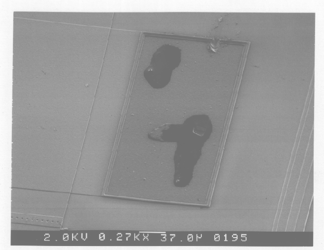
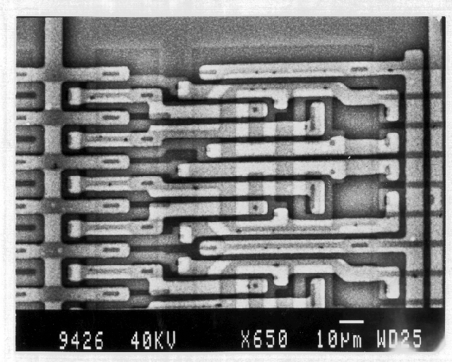
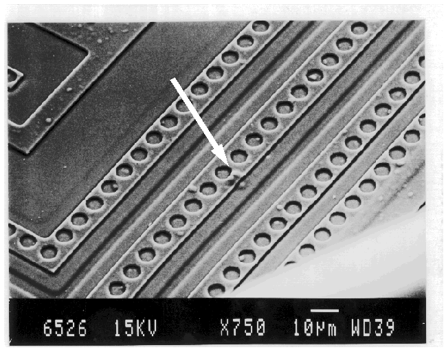
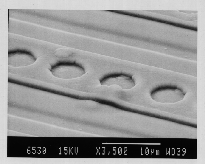
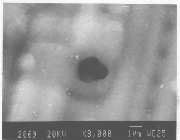
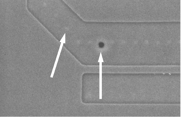
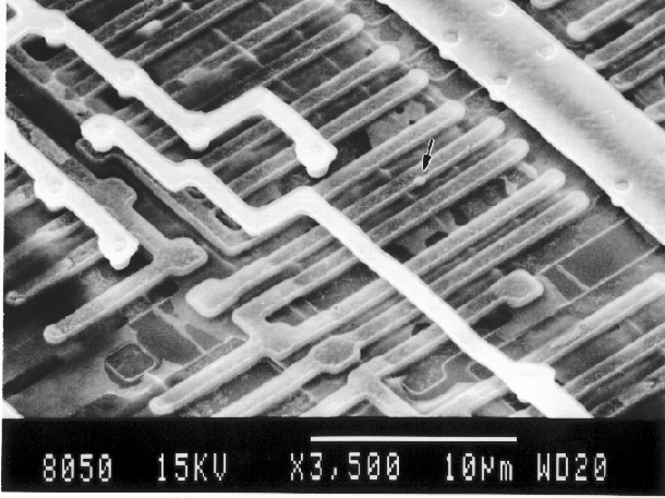
An SEM examination uses the scanning electron microscope to carefully examine the entire die surface in search of signs of mechanical damage, processing defects, dendrites, contamination, chipouts (portion of die missing), and/or cracks. The material below describes the basics of scanning electron microscopy.

Bond Wires

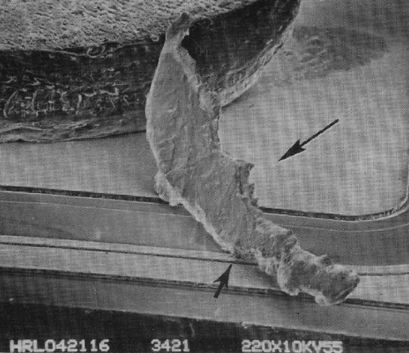
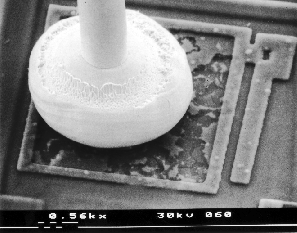
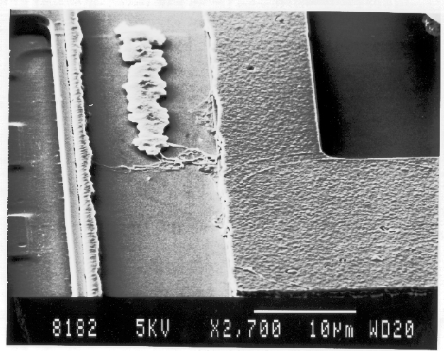
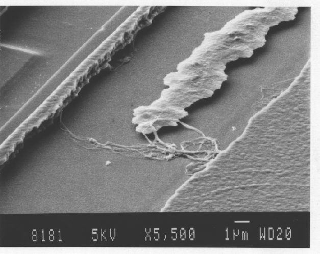
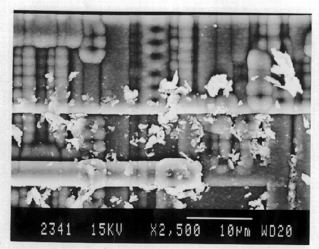
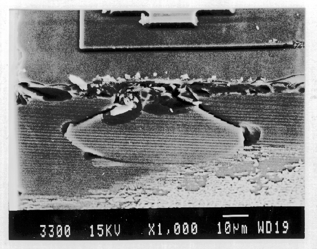
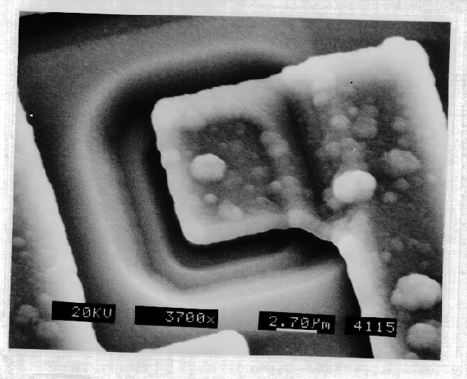
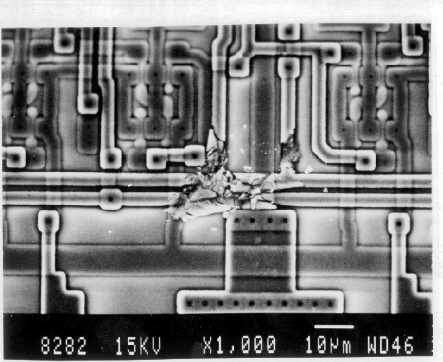
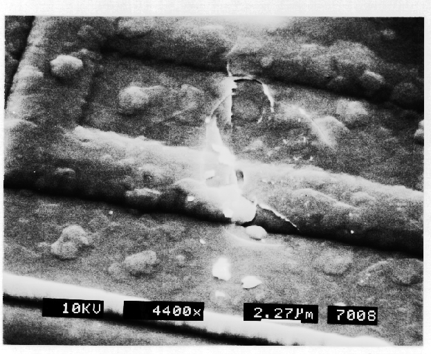
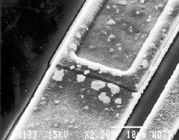
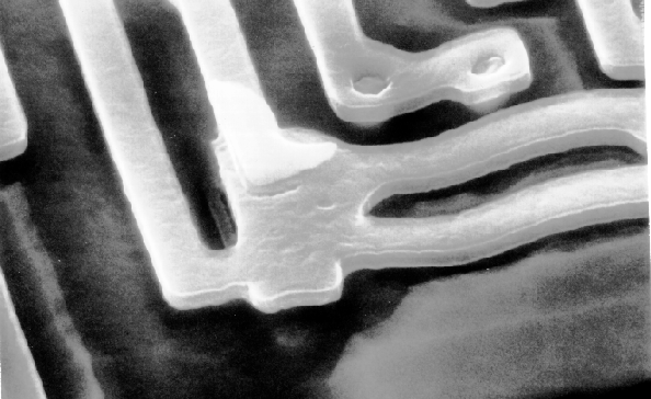
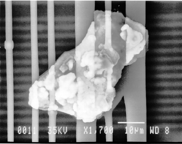
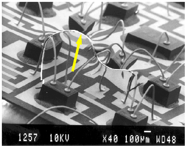
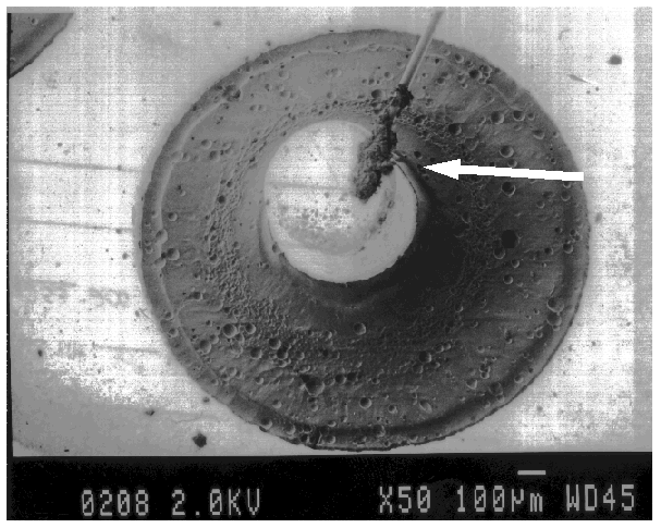
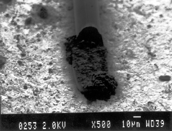
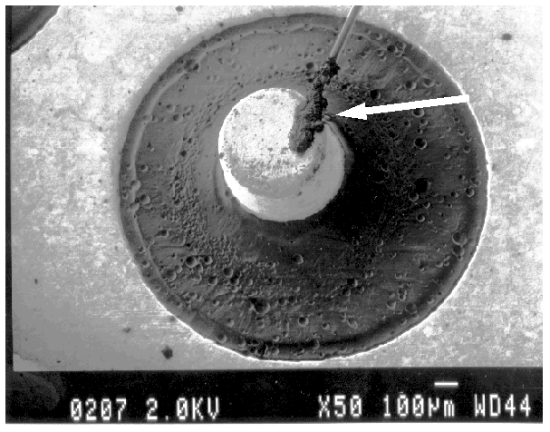
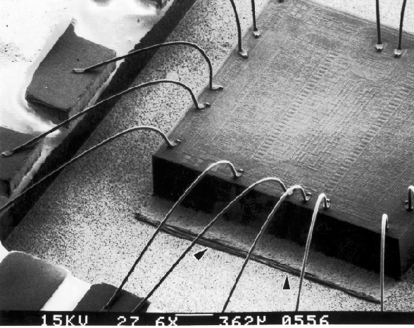
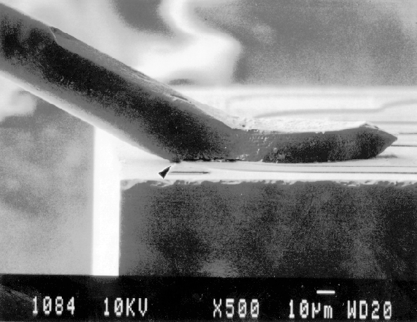
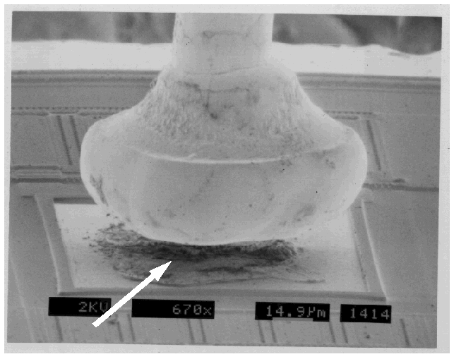
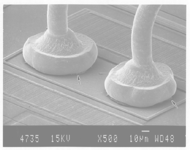
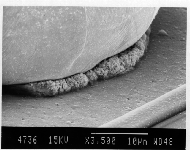
During an SEM bond wire examination, the analyst carefully scrutinizes the bond wire, the bond pads, and all surrounding areas for any anomalies, particulates, or contaminates. The SEM provides a high mag view of any questionable areas detected during optical evaluation.

IC Package

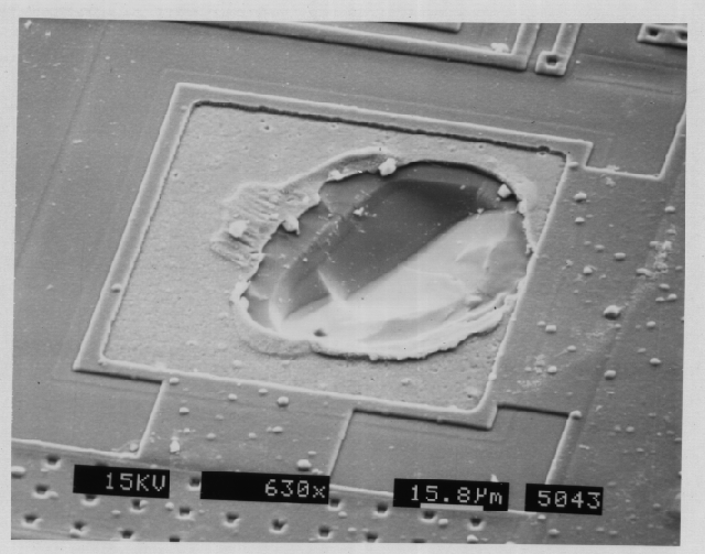
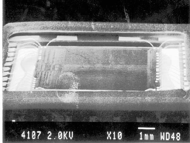
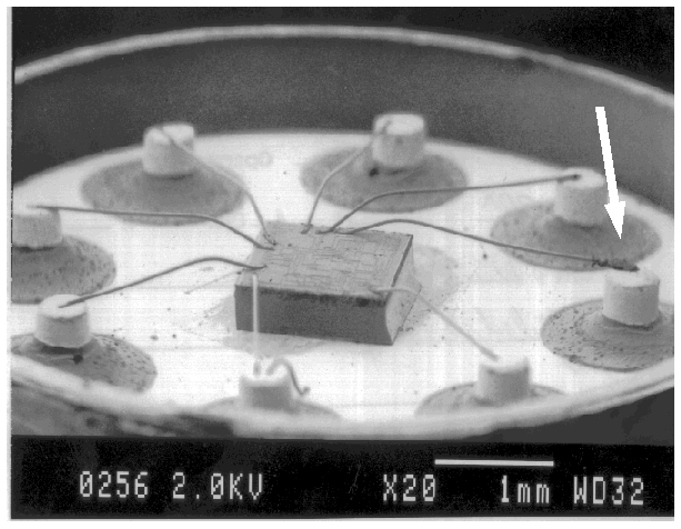
An SEM package examination is a careful examination of an IC package, which includes the lid seal area, the leads or pins, the lid, and the overall package.

Cross Section Examination

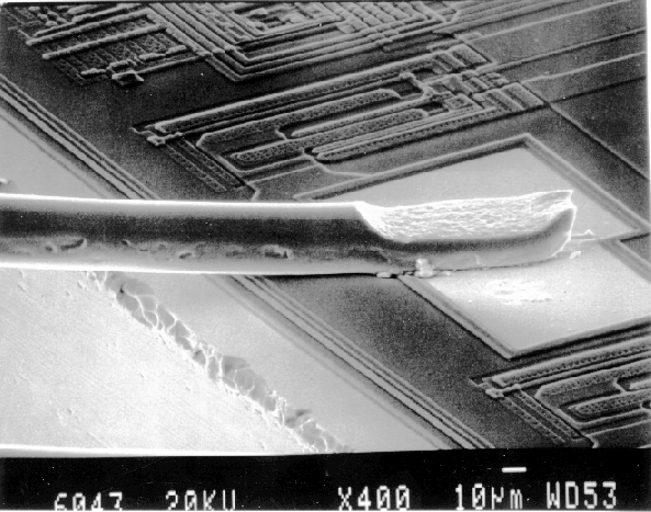
An SEM examination after cross sectioning is used to gather cross sectional information exposed by mechanically cross sectioning the IC or wafer or cross sectional information exposed by using a focused ion beam to cross section the IC. The SEM can yield important information concerning the processing of the IC, including feature sizes, thicknesses of layers, step coverage, etc.

Why Perform an SEM Die Examination?

Die

An SEM die examination should be performed whenever questions about the die condition cannot be verified using high mag optical examination.

Bond Wires

An SEM bond wire examination should be performed whenever a possible bond wire anomaly is suspected but cannot be verified with optical microscopy. The SEM can provide greater spatial resolution and greater depth of field than an optical microscope.

IC Package

This examination would usually be performed after the high mag optical examination where a possible abnormality was detected but could not be verified.

Cross Section Examination

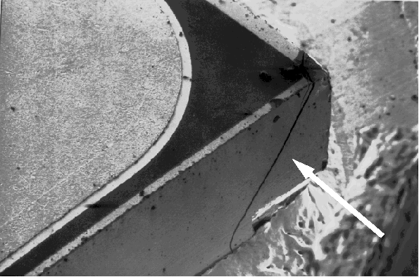
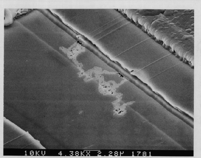
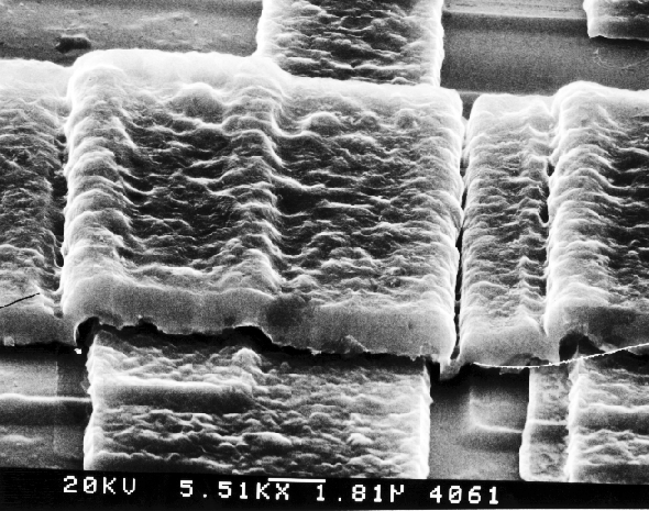
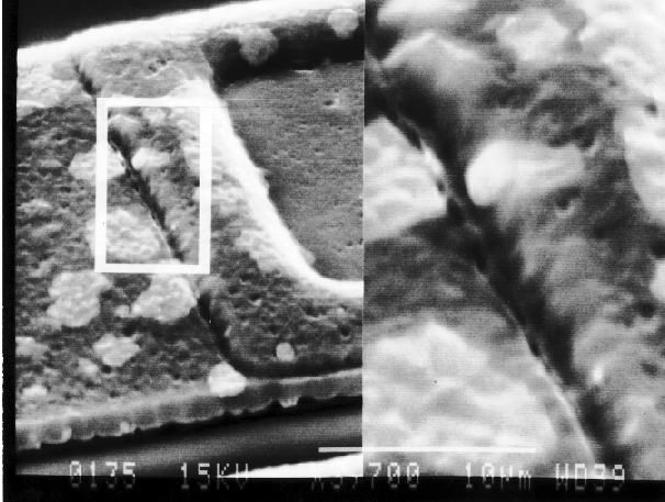
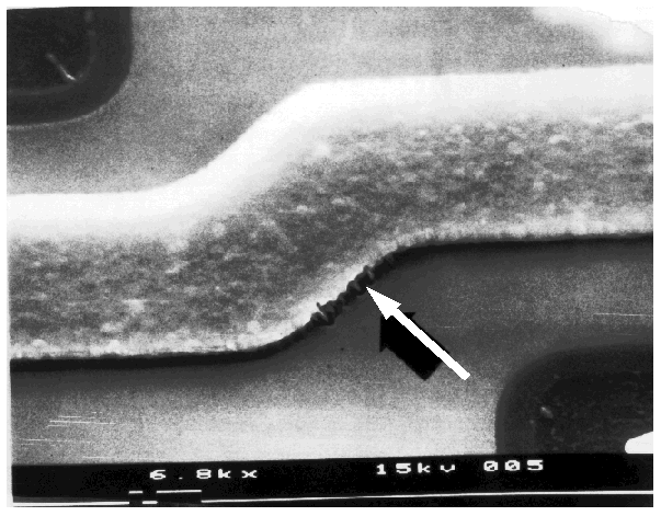
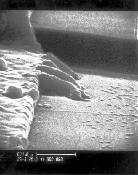
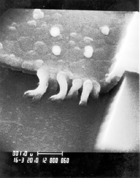
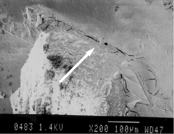
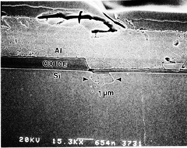
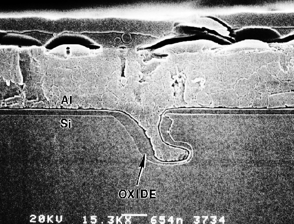
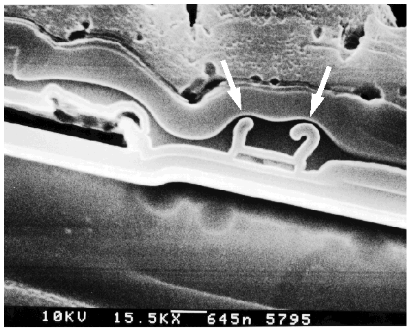
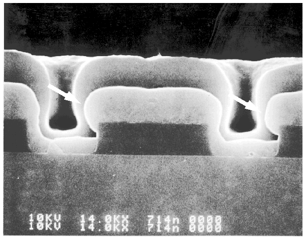
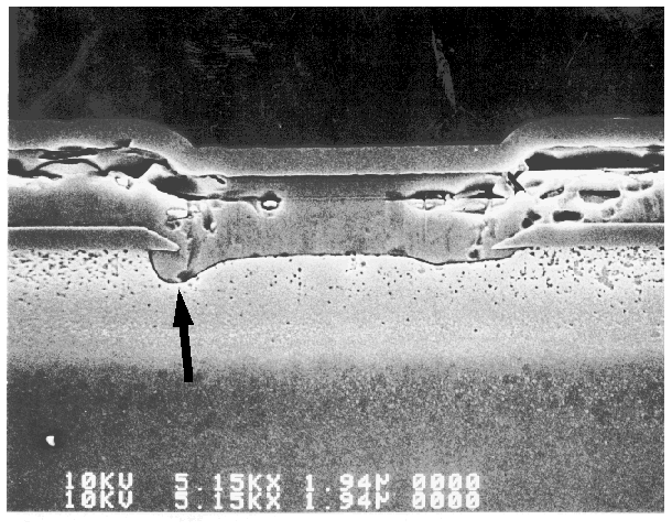
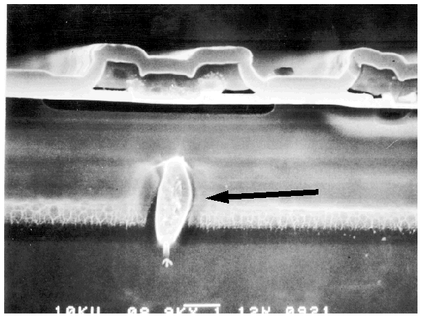
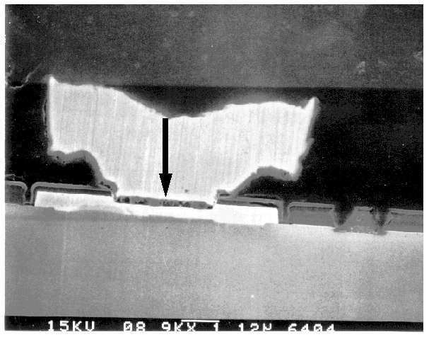
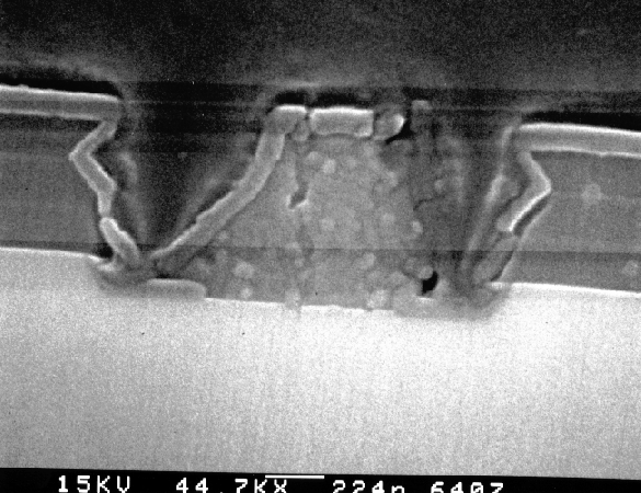
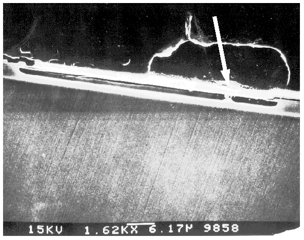
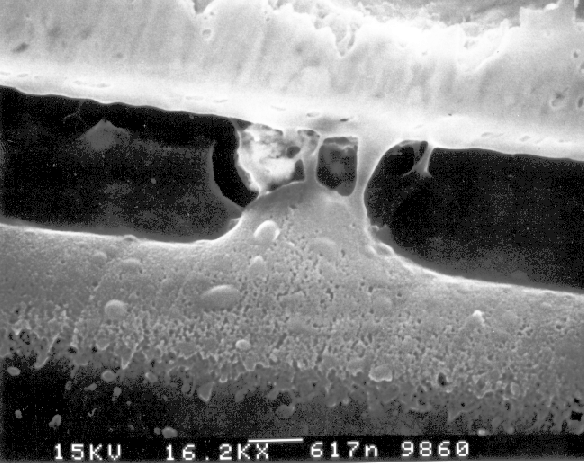
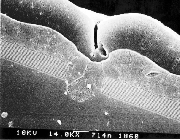
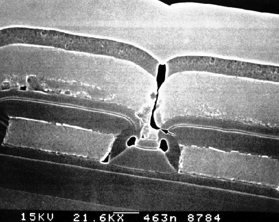
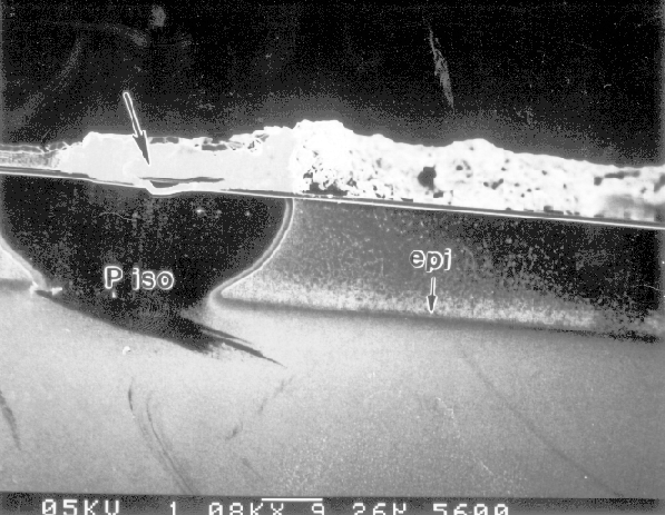
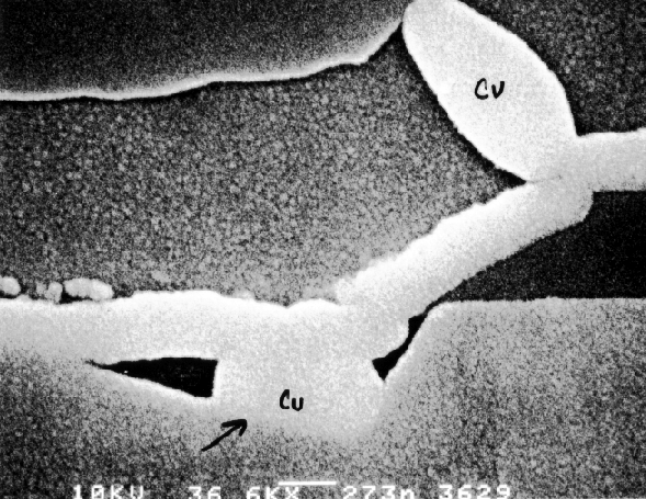
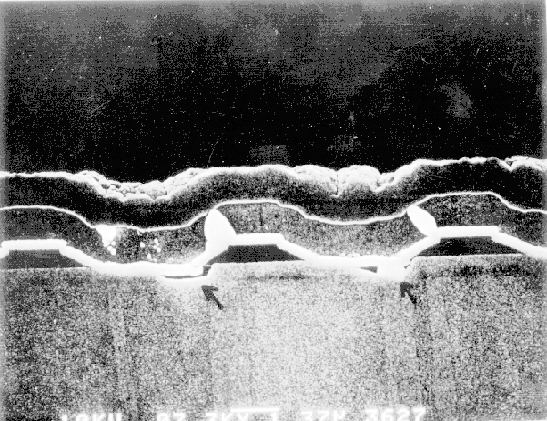
An SEM examination of the cross sectioned surface is important because the SEM is the normally the best tool the failure analyst can use to examine a cross sectioned surface. The spatial resolution of the SEM, coupled with its large depth of field and capability to perform elemental analysis, make it the tool of choice for most cross sections. The Focused Ion Beam (FIB), while potentially providing better contrast for some cross sectional information, is not always available and does not possess the spatial resolution of a standard SEM; additionally, the FIB is much more expensive.

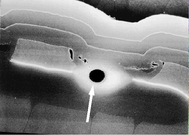
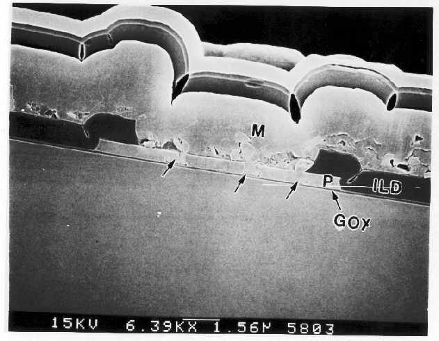
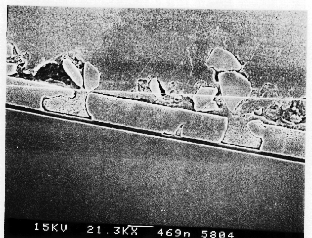
An SEM examination of the cross sectioned surface allows the analyst to identify poor step coverage, misalignment of various layers, voiding, incorrect thicknesses, and a host of other potential failure mechanisms.

How is an SEM Die Examination Performed?

Die

Select an accelerating voltage which will allow the least amount of charging while obtaining the best resolution. If the device is to be tested after the SEM examination, select the accelerating voltage carefully so that the electron beam does not damage the device. Scan the die. If step coverage is a significant factor, then the sample should be tilted to allow easy observation of the metal steps. If metal voiding is of concern, use the backscattered electron detector. (Note: If a barrier metal is used under the conductors, then the backscattered electron detector should not be used.) If contamination is observed or suspected, use the EDX detector to identify the contamination.

Bond Wires

Using a beam energy of 20 to 25 KV, carefully examine the suspect bond wire from the bond pad to the package lead. Pay attention to any anomalies, such as open wires, particles, contamination, a scribe line short, excessive wire height, and reverse bonded or previously bonded wires.

IC Package

Select an accelerating voltage that will allow the least amount of charging. Because the packages are usually made from a non-conducting material, e-beam charging can potentially inhibit analysis. If charging will not allow a complete analysis, coat the package with carbon or Au/Pd.

Cross Section Examination

For help on how to operate a scanning electron microscope, consult your operator's manual. To examine a cross sectioned sample, be sure to use an SEM where you can achieve a fairly large tilt angle ( >45° ). If the sample is mounted in an epoxy resin (from mechanical cross sectioning), be sure to clean the sample and vacuum bake to remove any contamination/moisture. Performing these steps facilitates a faster pump-down.

Before placing the sample in the SEM, you may desire to place fiduciary marks near the area of interest so that you can quickly locate the defect. This step is especially important on large memory ICs where the structures are repetitive and difficult to follow. If you are using a field emission SEM, try examining the IC at a low accelerating voltage (~ 1kV) without coating the sample. The spatial resolution should enable you to see nearly everything. If you are using a standard tungsten or LaB6 system, you will probably need to coat the sample and use a higher accelerating voltage (~ 10kV or higher) to encourage higher resolution.

When is an SEM Examination Performed?

Die

An SEM die examination would usually be performed after all other testing of the device is complete. The SEM analysis is considered non-destructive; however, the SEM will deposit a thin carbon layer on the sample when the beam scans the surface.

Bond Wires

Perform an SEM bond wire examination whenever a lead or bond wire anomaly is suspected but cannot be verified by high mag optical examination.

IC Package

An SEM package examination can be performed whenever potentially serious abnormalities, such as contamination, cracks, chips, or any defects, have been detected.

Cross Section Examination

An SEM examination of the cross sectioned surface should be performed immediately after you have finished the cross section and have determined optically that you have sectioned to the appropriate location. If you have placed the IC in the SEM and discovered you have not yet reached the area of interest, continue polishing on a mechanical cross sectioning wheel or remove additional material using the FIB.


References on SEM Die Examination

  1. Microelectronics Failure Analysis Techniques: A Procedural Guide, eds. Ed Doyle Jr. and Bill Morris, IITRI, 1980
  2. John R. Devany, Gerald L. Hill, and Robert G. Seippel, Failure Analysis Mechanisms, Techniques and Photo Atlas, Failure Recognition and Training Services, Inc. Monrovia CA. 1986

Die

SEM image showing contamination bridging between a bond wire and the substrate. (Photo courtesy DM Data.). SEM image showing contamination bridging between a bond wire and the substrate. (Photo courtesy DM Data.).
Figure 1. SEM image showing contamination bridging between a bond wire and the substrate. (Photo courtesy DM Data.).
SEM image showing corrosion on the bond pad. (Photo courtesy DM Data.). SEM image showing corrosion on the bond pad. (Photo courtesy DM Data.).
Figure 2. SEM image showing corrosion on the bond pad. (Photo courtesy DM Data.).
SEM image showing dendritic growth. (Photo courtesy Analytical Solutions.). SEM image showing dendritic growth. (Photo courtesy Analytical Solutions.).
Figure 3. SEM image showing dendritic growth. (Photo courtesy Analytical Solutions.).
SEM image showing dendritic growth at higher magnifications. (Photo courtesy Analytical Solutions.). SEM image showing dendritic growth at higher magnifications. (Photo courtesy Analytical Solutions.).
Figure 4. SEM image showing dendritic growth at higher magnifications. (Photo courtesy Analytical Solutions.).
SEM image showing a cracked die. (Photo courtesy Analytical Solutions.). SEM image showing a cracked die. (Photo courtesy Analytical Solutions.).
Figure 5. SEM image showing a cracked die. (Photo courtesy Analytical Solutions.).
SEM image showing contamination on a bond pad. (Photo courtesy DM Data.). SEM image showing contamination on a bond pad. (Photo courtesy DM Data.).
Figure 6. SEM image showing contamination on a bond pad. (Photo courtesy DM Data.).
SEM image showing particulate contamination on the die surface. (Photo courtesy Analytical Solutions.). SEM image showing particulate contamination on the die surface. (Photo courtesy Analytical Solutions.).
Figure 7. SEM image showing particulate contamination on the die surface. (Photo courtesy Analytical Solutions.).
SEM image showing a cracked die. Crack propagates into the substrate. (Photo courtesy Analytical Solutions). SEM image showing a cracked die. Crack propagates into the substrate. (Photo courtesy Analytical Solutions).
Figure 8. SEM image showing a cracked die. Crack propagates into the substrate. (Photo courtesy Analytical Solutions).
SEM image showing voiding in the metal. (Photo courtesy Analytical Solutions). SEM image showing voiding in the metal. (Photo courtesy Analytical Solutions).
Figure 9. SEM image showing voiding in the metal. (Photo courtesy Analytical Solutions).
SEM image showing a metal to silicon contact. (Photo courtesy Analytical Solutions). SEM image showing a metal to silicon contact. (Photo courtesy Analytical Solutions).
Figure 10. SEM image showing a metal to silicon contact. (Photo courtesy Analytical Solutions).
SEM image showing galvanic corrosion. (Photo courtesy Analytical Solutions). SEM image showing galvanic corrosion. (Photo courtesy Analytical Solutions).
Figure 11. SEM image showing galvanic corrosion. (Photo courtesy Analytical Solutions).
SEM image showing subtle electrical overstress damage. (Photo courtesy Analytical Solutions). SEM image showing subtle electrical overstress damage. (Photo courtesy Analytical Solutions).
Figure 12. SEM image showing subtle electrical overstress damage. (Photo courtesy Analytical Solutions).
SEM image showing Fig. 12 at higher magnification. (Photo courtesy Analytical Solutions). SEM image showing Fig. 12 at higher magnification. (Photo courtesy Analytical Solutions).
Figure 13. SEM image showing Fig. 12 at higher magnification. (Photo courtesy Analytical Solutions).
SEM image showing bond pad cratering. (Photo courtesy DM Data). SEM image showing bond pad cratering. (Photo courtesy DM Data).
Figure 14. SEM image showing bond pad cratering. (Photo courtesy DM Data).
SEM image showing damage caused by a blunt mechanical object. (Photo courtesy Analytical Solutions). SEM image showing damage caused by a blunt mechanical object. (Photo courtesy Analytical Solutions).
Figure 15. SEM image showing damage caused by a blunt mechanical object. (Photo courtesy Analytical Solutions).
SEM image showing cracks in the glass caused by electromigration. (Photo courtesy DM Data). SEM image showing cracks in the glass caused by electromigration. (Photo courtesy DM Data).
Figure 16. SEM image showing cracks in the glass caused by electromigration. (Photo courtesy DM Data).
SEM image showing a pin hole in the top glass layer. (Photo courtesy Analytical Solutions). SEM image showing a pin hole in the top glass layer. (Photo courtesy Analytical Solutions).
Figure 17. SEM image showing a pin hole in the top glass layer. (Photo courtesy Analytical Solutions).
SEM image showing thinning at steps, poor step coverage. (Photo courtesy DM Data). SEM image showing thinning at steps, poor step coverage. (Photo courtesy DM Data).
Figure 18. SEM image showing thinning at steps, poor step coverage. (Photo courtesy DM Data).
SEM image showing an electron channeling pattern. (Photo courtesy Analytical Solutions). SEM image showing an electron channeling pattern. (Photo courtesy Analytical Solutions).
Figure 19. SEM image showing an electron channeling pattern. (Photo courtesy Analytical Solutions).
SEM image showing copper leaching out on alumimun metal line as a result of moisture. (Photo courtesy Analytical Solutions). SEM image showing copper leaching out on alumimun metal line as a result of moisture. (Photo courtesy Analytical Solutions).
Figure 20. SEM image showing copper leaching out on alumimun metal line as a result of moisture. (Photo courtesy Analytical Solutions).
EM image showing copper leaching out on an aluminum metal line at higher magnification. (Photo courtesy Analytical Solutions). EM image showing copper leaching out on an aluminum metal line at higher magnification. (Photo courtesy Analytical Solutions).
Figure 21. EM image showing copper leaching out on an aluminum metal line at higher magnification. (Photo courtesy Analytical Solutions).
SEM image showing a gate oxide short at edge of poly line. (Photo courtesy Analytical Solutions). SEM image showing a gate oxide short at edge of poly line. (Photo courtesy Analytical Solutions).
Figure 22. SEM image showing a gate oxide short at edge of poly line. (Photo courtesy Analytical Solutions).
SEM image showing gate oxide short at edge of poly line. (Photo courtesy Analytical Solutions). SEM image showing gate oxide short at edge of poly line. (Photo courtesy Analytical Solutions).
Figure 23. SEM image showing gate oxide short at edge of poly line. (Photo courtesy Analytical Solutions).
SEM image showing gate oxide short at edge of poly line - different angle. (Photo courtesy Analytical Solutions). SEM image showing gate oxide short at edge of poly line - different angle. (Photo courtesy Analytical Solutions).
Figure 24. SEM image showing gate oxide short at edge of poly line - different angle. (Photo courtesy Analytical Solutions).
SEM image showing gate oxide short sites after poly removal. (Photo courtesy Analytical Solutions). SEM image showing gate oxide short sites after poly removal. (Photo courtesy Analytical Solutions).
Figure 25. SEM image showing gate oxide short sites after poly removal. (Photo courtesy Analytical Solutions).
SEM image showing metal 1 bridging short after metal 2 metal 1 interlevel dielectric layer removal. (Photo courtesy Analytical Solutions). SEM image showing metal 1 bridging short after metal 2 metal 1 interlevel dielectric layer removal. (Photo courtesy Analytical Solutions).
Figure 26. SEM image showing metal 1 bridging short after metal 2 metal 1 interlevel dielectric layer removal. (Photo courtesy Analytical Solutions).
SEM image showing titanium-tungsten particle bridging several metal 3 lines. (Photo courtesy Sandia Labs). SEM image showing titanium-tungsten particle bridging several metal 3 lines. (Photo courtesy Sandia Labs).
Figure 27. SEM image showing titanium-tungsten particle bridging several metal 3 lines. (Photo courtesy Sandia Labs).
SEM image showing a gate oxide defect before poly removal. (Photo courtesy Sandia Labs). SEM image showing a gate oxide defect before poly removal. (Photo courtesy Sandia Labs).
Figure 28. SEM image showing a gate oxide defect before poly removal. (Photo courtesy Sandia Labs).

Bond Wires

SEM image of magnetic particle bridging bond wires in a hybrid microcircuit. (Courtesy DM Data). SEM image of magnetic particle bridging bond wires in a hybrid microcircuit. (Courtesy DM Data).
Figure 29. SEM image of magnetic particle bridging bond wires in a hybrid microcircuit. (Courtesy DM Data).
SEM image of properly bonded wires in a static RAM. (Courtesy Analytical Solutions). SEM image of properly bonded wires in a static RAM. (Courtesy Analytical Solutions).
Figure 30. SEM image of properly bonded wires in a static RAM. (Courtesy Analytical Solutions).
SEM image of contamination on a bond wire. (Courtesy DM Data). SEM image of contamination on a bond wire. (Courtesy DM Data).
Figure 31. SEM image of contamination on a bond wire. (Courtesy DM Data).
SEM image of bond wire that is not making connection to the bond pad as evidenced by bond wire charging positively, blurring the image. (Courtesy Analytical Solutions). SEM image of bond wire that is not making connection to the bond pad as evidenced by bond wire charging positively, blurring the image. (Courtesy Analytical Solutions).
Figure 32. SEM image of bond wire that is not making connection to the bond pad as evidenced by bond wire charging positively, blurring the image. (Courtesy Analytical Solutions).
SEM image of contamination on a bond wire in an operational amplifier. (Courtesy DM Data). SEM image of contamination on a bond wire in an operational amplifier. (Courtesy DM Data).
Figure 33. SEM image of contamination on a bond wire in an operational amplifier. (Courtesy DM Data).
SEM image of extra bond wire material in the package cavity. (Courtesy DM Data). SEM image of extra bond wire material in the package cavity. (Courtesy DM Data).
Figure 34. SEM image of extra bond wire material in the package cavity. (Courtesy DM Data).
SEM image of contamination on a bond wire in an operational amplifier. (Courtesy DM Data). SEM image of contamination on a bond wire in an operational amplifier. (Courtesy DM Data).
Figure 35. SEM image of contamination on a bond wire in an operational amplifier. (Courtesy DM Data).
SEM image of bond wire with a low take off angle, most likely reverse bonded. (Courtesy DM Data). SEM image of bond wire with a low take off angle, most likely reverse bonded. (Courtesy DM Data).
Figure 36. SEM image of bond wire with a low take off angle, most likely reverse bonded. (Courtesy DM Data).
SEM image of a bond wire shorting to the die scribeline. (Courtesy Analytical Solutions). SEM image of a bond wire shorting to the die scribeline. (Courtesy Analytical Solutions).
Figure 37. SEM image of a bond wire shorting to the die scribeline. (Courtesy Analytical Solutions).
SEM image of intermetallics on bond pad. (Courtesy DM Data). SEM image of intermetallics on bond pad. (Courtesy DM Data).
Figure 38. SEM image of intermetallics on bond pad. (Courtesy DM Data).
SEM image showing intermetallic growth on two bond wire/bond pad interfaces. (Courtesy Analytical Solutions). SEM image showing intermetallic growth on two bond wire/bond pad interfaces. (Courtesy Analytical Solutions).
Figure 39. SEM image showing intermetallic growth on two bond wire/bond pad interfaces. (Courtesy Analytical Solutions).
High magnification image of intermetallic growth. (Courtesy DM Data). High magnification image of intermetallic growth. (Courtesy DM Data).
Figure 40. High magnification image of intermetallic growth. (Courtesy DM Data).
Figure of bond wire sheared off at heel as a result of improper operation of the wire bond tool. (Courtesy DM Data). Figure of bond wire sheared off at heel as a result of improper operation of the wire bond tool. (Courtesy DM Data).
Figure 41. Figure of bond wire sheared off at heel as a result of improper operation of the wire bond tool. (Courtesy DM Data).
SEM image of bond wire crack just above ball. (Courtesy DM Data). SEM image of bond wire crack just above ball. (Courtesy DM Data).
Figure 42. SEM image of bond wire crack just above ball. (Courtesy DM Data).

IC Package

SEM image showing cracking at lead interface to package. (Courtesy DM Data). SEM image showing cracking at lead interface to package. (Courtesy DM Data).
Figure 43. SEM image showing cracking at lead interface to package. (Courtesy DM Data).
SEM image showing contamination bridging two leads on a package. (Courtesy DM Data). SEM image showing contamination bridging two leads on a package. (Courtesy DM Data).
Figure 44. SEM image showing contamination bridging two leads on a package. (Courtesy DM Data).
High magnification SEM image showing cracking at lead interface to package. (Courtesy DM Data). High magnification SEM image showing cracking at lead interface to package. (Courtesy DM Data).
Figure 45. High magnification SEM image showing cracking at lead interface to package. (Courtesy DM Data).

Cross Section Examination

SEM image showing etching pit into the Si substrate as a result of a breach in the overlying oxide layer. (Courtesy Analytical Solutions). SEM image showing etching pit into the Si substrate as a result of a breach in the overlying oxide layer. (Courtesy Analytical Solutions).
Figure 46. SEM image showing etching pit into the Si substrate as a result of a breach in the overlying oxide layer. (Courtesy Analytical Solutions).
SEM image showing a different etching pit into the Si substrate. Note that oxide and Al were both deposited into the pit indicating that the etched pit occurred early in processing. (Courtesy Analytical Solutions). SEM image showing a different etching pit into the Si substrate. Note that oxide and Al were both deposited into the pit indicating that the etched pit occurred early in processing. (Courtesy Analytical Solutions).
Figure 47. SEM image showing a different etching pit into the Si substrate. Note that oxide and Al were both deposited into the pit indicating that the etched pit occurred early in processing. (Courtesy Analytical Solutions).
SEM image showing oxide whiskers due to incorrect processing and composition. (Courtesy Analytical Solutions). SEM image showing oxide whiskers due to incorrect processing and composition. (Courtesy Analytical Solutions).
Figure 48. SEM image showing oxide whiskers due to incorrect processing and composition. (Courtesy Analytical Solutions).
SEM image showing poor step coverage (breadloafing) of metal 1 into a silicon contact. (Courtesy Analytical Solutions). SEM image showing poor step coverage (breadloafing) of metal 1 into a silicon contact. (Courtesy Analytical Solutions).
Figure 49. SEM image showing poor step coverage (breadloafing) of metal 1 into a silicon contact. (Courtesy Analytical Solutions).
SEM image showing overetched contact windows that undercut the field oxide. (Courtesy Analytical Solutions). SEM image showing overetched contact windows that undercut the field oxide. (Courtesy Analytical Solutions).
Figure 50. SEM image showing overetched contact windows that undercut the field oxide. (Courtesy Analytical Solutions).
SEM image showing damage result from a collector to emitter short on a bipolar IC. (Courtesy Analytical Solutions). SEM image showing damage result from a collector to emitter short on a bipolar IC. (Courtesy Analytical Solutions).
Figure 51. SEM image showing damage result from a collector to emitter short on a bipolar IC. (Courtesy Analytical Solutions).
SEM image showing an open metal 1 - metal 2 contact. Oxide not fully removed from contact area. (Courtesy Analytical Solutions). SEM image showing an open metal 1 - metal 2 contact. Oxide not fully removed from contact area. (Courtesy Analytical Solutions).
Figure 52. SEM image showing an open metal 1 - metal 2 contact. Oxide not fully removed from contact area. (Courtesy Analytical Solutions).
SEM image showing an overetched metal1 - Si contact and poor oxide coverage. (Courtesy Analytical Solutions). SEM image showing an overetched metal1 - Si contact and poor oxide coverage. (Courtesy Analytical Solutions).
Figure 53. SEM image showing an overetched metal1 - Si contact and poor oxide coverage. (Courtesy Analytical Solutions).
SEM image showing a metal to substrate short on a capacitor on a bipolar IC. (Courtesy Analytical Solutions). SEM image showing a metal to substrate short on a capacitor on a bipolar IC. (Courtesy Analytical Solutions).
Figure 54. SEM image showing a metal to substrate short on a capacitor on a bipolar IC. (Courtesy Analytical Solutions).
Higher magnification image of the metal to substrate short. (Courtesy Analytical Solutions). Higher magnification image of the metal to substrate short. (Courtesy Analytical Solutions).
Figure 55. Higher magnification image of the metal to substrate short. (Courtesy Analytical Solutions).
SEM image showing breach in the field oxide, resulting in a metal to silicon short. (Courtesy Analytical Solutions). SEM image showing breach in the field oxide, resulting in a metal to silicon short. (Courtesy Analytical Solutions).
Figure 56. SEM image showing breach in the field oxide, resulting in a metal to silicon short. (Courtesy Analytical Solutions).
SEM image showing open metal interconnect at a step due to lack of step coverage. (Courtesy Analytical Solutions). SEM image showing open metal interconnect at a step due to lack of step coverage. (Courtesy Analytical Solutions).
Figure 57. SEM image showing open metal interconnect at a step due to lack of step coverage. (Courtesy Analytical Solutions).
SEM image showing processing defect over the p isolation region, resulting in a short. (Courtesy Analytical Solutions). SEM image showing processing defect over the p isolation region, resulting in a short. (Courtesy Analytical Solutions).
Figure 58. SEM image showing processing defect over the p isolation region, resulting in a short. (Courtesy Analytical Solutions).
SEM image showing excess copper in metallization system causing short. (Courtesy Analytical Solutions). SEM image showing excess copper in metallization system causing short. (Courtesy Analytical Solutions).
Figure 59. SEM image showing excess copper in metallization system causing short. (Courtesy Analytical Solutions).
Lower magnification image showing location of shorts due to excess copper in metallization system. (Courtesy Analytical Solutions). Lower magnification image showing location of shorts due to excess copper in metallization system. (Courtesy Analytical Solutions).
Figure 60. Lower magnification image showing location of shorts due to excess copper in metallization system. (Courtesy Analytical Solutions).
SEM image showing void in die attach. (Courtesy Analytical Solutions). SEM image showing void in die attach. (Courtesy Analytical Solutions).
Figure 61. SEM image showing void in die attach. (Courtesy Analytical Solutions).
SEM image showing gap between lead and leadframe (potential entry point for moisture or other volatiles). (Courtesy Analytical Solutions). SEM image showing gap between lead and leadframe (potential entry point for moisture or other volatiles). (Courtesy Analytical Solutions).
Figure 62. SEM image showing gap between lead and leadframe (potential entry point for moisture or other volatiles). (Courtesy Analytical Solutions).
Lower magnification image of the lead and leadframe. (Courtesy Analytical Solutions). Lower magnification image of the lead and leadframe. (Courtesy Analytical Solutions).
Figure 63. Lower magnification image of the lead and leadframe. (Courtesy Analytical Solutions).
SEM image showing collector to emitter damage on a pnp transistor on a bipolar IC. (Courtesy Analytical Solutions). SEM image showing collector to emitter damage on a pnp transistor on a bipolar IC. (Courtesy Analytical Solutions).
Figure 64. SEM image showing collector to emitter damage on a pnp transistor on a bipolar IC. (Courtesy Analytical Solutions).
SEM image showing blown fusible link on a read only memory. (Courtesy Analytical Solutions). SEM image showing blown fusible link on a read only memory. (Courtesy Analytical Solutions).
Figure 65. SEM image showing blown fusible link on a read only memory. (Courtesy Analytical Solutions).
SEM image showing aluminum inclusions in a polysilicon gate resulting in a shorted transistor. (Courtesy Analytical Solutions). SEM image showing aluminum inclusions in a polysilicon gate resulting in a shorted transistor. (Courtesy Analytical Solutions).
Figure 66. SEM image showing aluminum inclusions in a polysilicon gate resulting in a shorted transistor. (Courtesy Analytical Solutions).
Higher magnification image of aluminum inclusions into the polysilicon gate. (Courtesy Analytical Solutions). Higher magnification image of aluminum inclusions into the polysilicon gate. (Courtesy Analytical Solutions).
Figure 67. Higher magnification image of aluminum inclusions into the polysilicon gate. (Courtesy Analytical Solutions).