System Maintenance occurs every Friday.
System Maintenance occurs every Friday.
Scanning Probe Microscopy is a series of techniques based on a class of new instruments that originated from the scanning tunneling microscope.
In 1981, researchers Gerd Binning and Heinrich Rohrer at the IBM Zurich Research Laboratory developed the scanning tunneling microscope, enabling imaging of conducting surfaces with atom scale resolution. Their invention received the Nobel Prize in Physics in 1986.
In the years following Binning and Rohrer's invention, many researchers have developed other systems based on the concept of the scanning tunneling microscope. Figure 1 describes many of the extensions that have been developed in recent years. Of the systems developed, several have recently become of interest to the failure analysis community. These systems include the atomic force microscope, the scanning capacitance probe microscope, the scanning thermal microscope, the magnetic force microscope, the scanning near-field optical microscope, and the scanning Kelvin force microscope. Each of these systems is discussed in detail below.
| Instrument | Developers | Capability | Year Developed |
|---|---|---|---|
| Scanning Tunneling Microscope | G. Binning, H. Rohrer | Atomic resolution images of conducting surfaces | 1981 |
| Scanning Near-Field Optical Microscope | D. W. Pohl | 50 nm (lateral resolution) optical images | 1982 |
| Scanning Capacitance Microscope | J. R. Matey, J. Blanc | 500 nm (lateral resolution) images of capacitance variation | 1984 |
| Scanning Thermal Microscope | C. C. Williams, H. K. Wickramasinghe | 50 nm (lateral resolution) thermal images | 1985 |
| Atomic Force Microscope | G. Binning, C. F. Quate, Ch. Gerber | Atomic resolution on conducting/non-conducting surfaces | 1986 |
| Scanning Attractive Force Microscope | Y. Martin, C. C. Williams, H. K. Wickramasinghe | 5 nm (lateral resolution) non-contact images of surfaces | 1987 |
| Magnetic Force Microscope | Y. Martin, H. K. Wickramasinghe | 100 nm (lateral resolution) of magnetic bits/heads | 1987 |
| Frictional Force Microscope | C. M. Mate, G. M. McClelland, S. Chiang | Atomic scale images of lateral (frictional) forces | 1987 |
| Electrostatic Force Microscope | Y. Martin, D. H. Abraham, H. K. Wickramasinghe | Detection of charge as small as a single electron | 1987 |
| Inelastic Tunneling Spectroscopy STM | D. P. E. Smith, D. Kirk, C. F. Quate | Phonon spectra of molecules in STM | 1987 |
| Laser Driven STM | L. Arnold, W. Krieger, H. Walther | Imaging by non-linear mixing of optical waves in STM | 1987 |
| Ballistic Electron Emission Microscope | W. J. Kaiser | Probing of Schottky barriers on nm scale | 1988 |
| Inverse Photoemission Force Microscope | J. H. Coombs, J. K. Gimzewski, B. Reihl, J. K. Sass, R. Schlittler | Luminescence spectra on nm scale | 1989 |
| Near Field Acoustic Microscope | K. Takata, T. Hasegawa, S. Hosaka, S. Hosoki, T. Komoda | Low frequency acoustic measurements on 10 nm scale | 1989 |
| Scanning Noise Microscope | R. Moller, A. Esslinger, B. Koslowski | Tunneling microscopy with zero tip-sample bias | 1989 |
| Scanning Spin-precession Microscope | Y. Manassen, R. Hamers, J. Demuth, A. Castellano | 1 nm (lateral resolution) images of paramagnetic spins | 1989 |
| Scanning Ion Conductance Microscope | P. Hansma, B. Drake, O. Marti. S. Gould, C. Prater | 500 nm (lateral resolution) images in electrolyte | 1989 |
| Scanning Electrochemical Microscope | O. E. Husser, D. H. Craston, A. J. Bard | 1989 | |
| Absorption Microscope/Spectroscope | J. Weaver, H. K. Wichramasinghe | 1 nm (lateral resolution absorption images/spectroscopy | 1989 |
| Phonon Absorption Microscope | H. K. Wickrama-singhe, J. Weaver, C. C. Williams | Phonon absorption images with nm resolution | 1989 |
| Scanning Chemical Potential Microscope | C. C. Williams, H. K. Wickramasinghe | Atomic scale images of chemical potential variation | 1990 |
| Photovoltage STM | R. J. Hamers, K. Markert | Photovoltage images on nm scale | 1990 |
| Kelvin Probe Force Microscope | M. Nonnenmacher, M. P. O'Boyle, H. K. Wickramasinghe | Contact potential measurements on 10 nm scale | 1991 |
The atomic force microscope is clearly the most popular of the scanning probe microscope techniques. It was developed by Gerd Binning, Christoph Gerber, and Calvin Quate in 1985. The system's atomically sharp tip resembles that of the scanning tunneling microscope. However, instead of measuring tunneling current between the tip and the sample, the atomic force microscope measures the repulsive force between the electron cloud of the tip and the electron cloud of the surface. This system advanced the ability to image the topography of insulating surfaces as well as conducting surfaces. The original atomic force microscope systems were contact mode systems, i.e., the tip was in contact with the sample surface. In newly designed non-contact mode systems, the tip can be scanned at a fixed distance from the sample surface.
Figure 2 illustrates the basic components of the atomic force microscope. The tip is scanned over the sample surface through the movement of three piezoelectric drivers: one for x motion, one for y motion, and one for z motion. Topography is measured by maintaining a constant force on the tip and adjusting the z-direction piezoelectric driver to compensate for topography changes. Shining a laser beam off a mirror mounted to the back of the cantilever and into a detector maintains the necessary constant force on the tip. As the topography changes, the cantilever will bend either up or down, causing the laser beam reflection to move. The piezoelectric driver will compensate to keep the laser beam aligned to the detector. The topography map is then generated from the changes in the piezoelectric driver. In the original system by Binning, Gerber, and Quate, a scanning tunneling tip in contact with the back surface of the AFM cantilever was used to provide feedback.


The soft cantilever spring makes the Atomic Force Microscope more sensitive than a stylus profilometer. AFM cantilevers are typically made from silicon, silicon oxide, or silicon nitride using standard photolithographic techniques. These photolithographic methods produce a cantilever with a spring constant of approximately 0.1 - 1.0 N/m--a value much less than the spring constant of a profilometer stylus. This spring constant is less than the interatomic spring constants, which are on the order of 10 N/m. This difference allows the AFM to measure angstrom-size displacements.
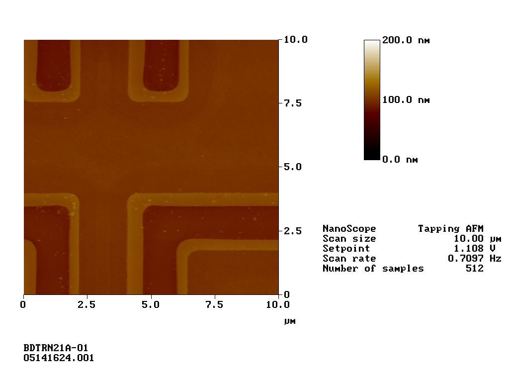
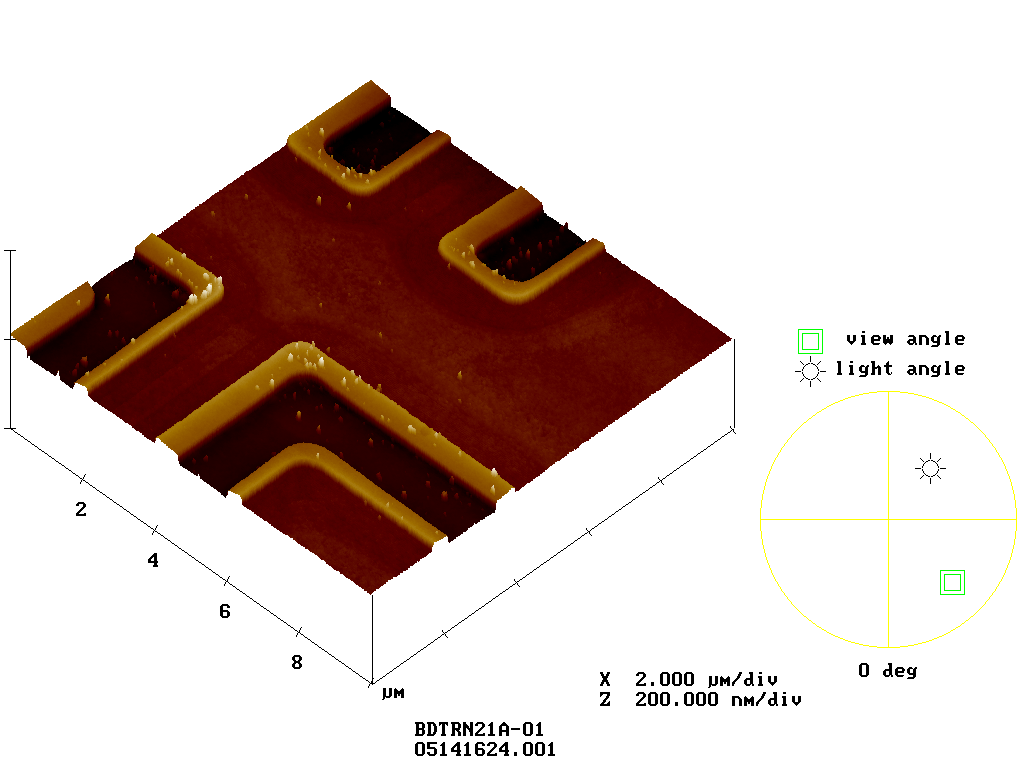
The scanning capacitance probe microscope is an extension of atomic force microscopy that is designed to measure carrier concentration. The scanning capacitance microscope relies on a UHF (Ultra High Frequency) Resonant Capacitance sensor connected to a conductive probe tip (see Figure 3). When the resonating probe tip is placed in contact with the IC surface, the sensor, transmission line, probe, and carriers in the sample near the tip all become part of the resonator. Consequently, tip-sample capacitance and variations will load the end of the transmission line and change the system's resonant frequency. Small changes in resonant frequency cause large changes in the resonance sensor output signal. Because of the resonance effect, this tip configuration is theoretically sensitive to variations of capacitance that are in the attofarad range (10-18 F).


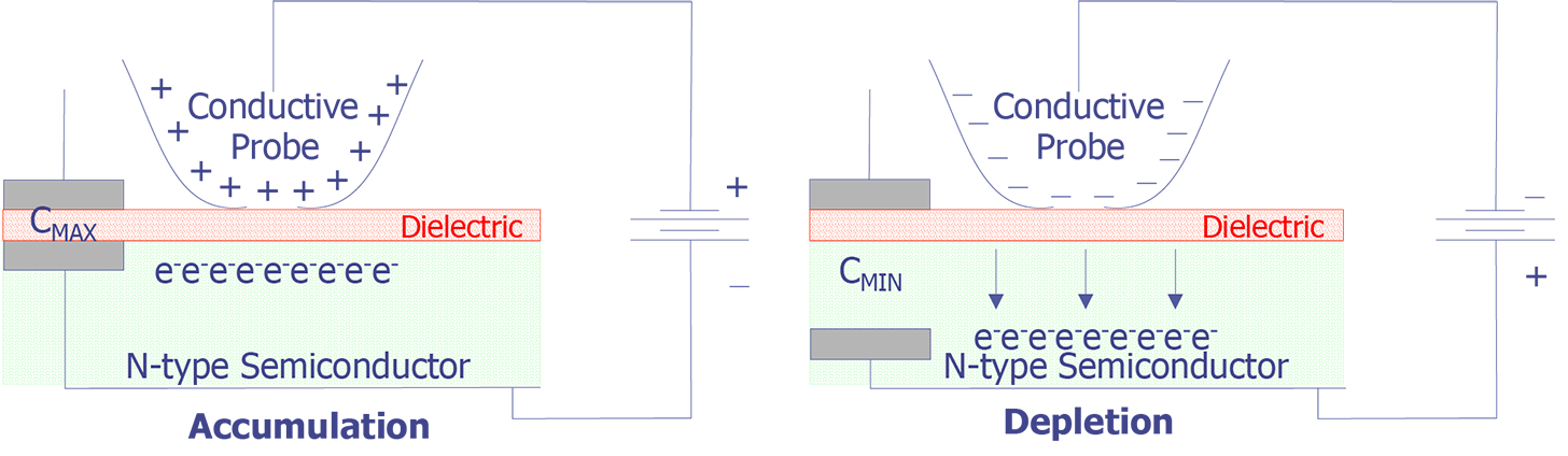
Applying an AC electric field between the tip and the sample generates capacitance variations. In order to produce an AC electric field, apply a kilohertz frequency AC bias voltage to the semiconductor material. Due to the resulting AC field, the free carriers in the sample beneath the grounded tip are alternately attracted or repulsed by the tip. The depletion and accumulation of carriers beneath the tip can be modeled as a capacitor with plates that vary in distance with respect to time (see Figure 4). The fluctuation in capacitance changes the resonant sensor system's capacitive load and resonant frequency. The strength of the applied field, the quality and thickness of the dielectric and the free carrier concentration govern the depth of the depletion layer. If the semiconductor material has uniform doping and differing thicknesses of overlying dielectric material, the depletion layer will be deeper under the thinner oxide regions. Similarly, in a sample that has varying carrier concentrations, the depletion in the low-concentration region will be deeper for the same applied voltage, and the amplitude of the capacitance charge generated by the AC bias would be higher in the same location.
Scanning Capacitance Microscopy measures the movement of carriers, which translates into a stronger signal for low carrier concentration and/or thin oxides. The signal can be expressed as dC/dV (the change in capacitance with respect to the change in applied voltage. In an AC condition, dV can be thought of as the peak-to-peak voltage, while dC can be thought of as proportional to the change in depletion depth of the semiconductor under the probe. One typically plots the relationship between capacitance and voltage on a C-V curve. In scanning capacitance microscopy, a constant amplitude sine wave voltage is applied to the sample; then, an image is constructed from the amplitude of the capacitance modulation. The DC bias to the sample can be adjusted, changing the AC bias point.
Probably the most common use of scanning capacitance microscopy is two-dimensional depth profiling. Because SIMS and C-V measurements only allow 1-dimensional measurements, scanning capacitance microscopy is viewed as a major step forward in understanding local device engineering.
Scanning Probe Microscopy can be most useful in making high resolution topographical measurements. In fact, many fabrication lines now use Atomic Force Microscopes in conjunction with other profilometers for metrology purposes.
For failure analysis applications, the ubiquity of the atomic force microscope will increase as defects that cause ICs to fail become smaller and smaller. The atomic force microscope can provide high resolution images of these defects. At this time, the atomic force microscope is the only widespread tool capable of examining defects smaller than 10 nm.
In the future, analysts may use the scanning probe microscope more frequently to sense heat, capacitance, current, electric field, and voltage. The SPM is capable of providing higher spatial resolution and superior sensitivity. For example, the SPM is capable of sensing voltages in the microvolt range.
Because it is essentially a surface science instrument, SPM has limited applicability. The SPM cannot effectively examine signals from interconnect or other structures that are buried beneath overlying conductors. In that sense, the SPM will be no more effective than electron beam probing. Magnetic current imaging using an SPM may be somewhat more useful. Computerized routines that can deconvolve signals may allow some use of magnetic force microscopy to measure current from buried interconnect.
Another factor that limits the acceptance of SPM is the image acquisition time, which can exceed several minutes. Most current ICs require observation of signals that occur in nanoseconds. It may be particularly difficult to observe real-time events using the SPM.
Overall, the SPM enables many techniques that exhibit its potential as an effective tool for failure analysis. Expect to see SPM techniques become more widely used in industry in the next five to ten years.
Most new Atomic Force Microscopes are much easier to use than the original research instruments created at many universities. Perform an AFM scan on an integrated circuit or sample by following these steps:
These steps are explained in detail below.
An AFM has three basic operation modes: contact mode, non-contact mode, and tapping mode. Tapping mode is a patented technique by Digital Instruments. In contact mode, the tip makes contact with the surface (or interacts in a regime dominated by near field forces). In non-contact mode, the tip does not make contact with the surface but is instead dominated by far field forces. To select the mode of operation on a Digital Instruments machine, set the AFM Mode to either tapping or contact in the Other Controls panel.
To mount the probe tip in the cantilever holder, use a magnifying lens or low power microscope and a pair of fine-tipped tweezers. Using the tweezers, grab a probe tip by the sides and place it on the cantilever holder. Be sure that the probe tip is in firm contact with the end of the groove. For tapping mode AFM, use an etched single crystal silicon probe; for contact mode AFM, use a silicon nitride probe. Once the probe tip is mounted to the cantilever holder, mount the holder onto the end of the scanner head.
Next, align the laser so that it is on the cantilever using the two screws on the top of the scanner. For tapping mode AFM, the SUM signal should be ~ 2 volts; for contact mode AFM, the SUM signal should be 4-6 volts.
Next, adjust the photodetector so that the red dot moves towards the center of the square. This can be done using the two screws on the side of the scanner. For tapping mode AFM, center the red dot and set the vertical deflection to a value close to 0 volts. For contact mode AFM, the horizontal deflection should be ~ 0 volts and the vertical deflection should be approximately -2 volts.
Next, locate the tip. Using the mouse, select Stage/Locate Tip. Center the tip on the cantilever under the cross hairs using the two adjustment screws to the left of the optical objective on the microscope. Focus on the tip end of the cantilever using the trackball while holding down the bottom left button. Next, focus on the surface of the sample. Select Stage/Focus Surface. The optics will move to a focus position ~ 1 mm below the tip. Focus on the sample surface by rolling the trackball up or down while pressing the bottom left button. This adjustment raises or lowers the vertical engage stage on which the SPM and optics are mounted. Ensure that the tip does not hit the sample surface. Move the desired measurement point under the cross hairs with the trackball without holding down any of the buttons. If you are performing tapping mode AFM, you will now need to tune the cantilever. Click on View/Cantilever Tune. For auto tune controls, make sure that the Start Frequency is at 100 kHz and the End Frequency is at 500 kHz. Target Amplitude should be between 2 and 3 volts. Click on Auto Tune. A "Tuning" message should appear and then disappear once the Auto Tune is done. When done, exit the Cantilever Tune control panel.
Next, set the initial scan parameters. In the Scan Controls panel, set the initial scan size to 1 µm, the X and Y offsets to 0, and the scan angle to 0.
Open the Feedback Controls menu. For tapping mode AFM, set the integral gain to 0.5, the proportional gain to 0.7, and the scan rate to 2 Hz. For contact mode AFM, set the setpoint to 0 volts, the integral gain to 2.0, the proportional gain to 3.0, and the scan rate to 2 hertz. You should now be ready to engage the drive motors for imaging.
Next, engage the scan motors by clicking on the Motor Engage menu item. For tapping mode, select View/Scope Mode. Check to see if Trace and Retrace are tracking correctly. If they are tracking, the lines should look the same, but they will not necessarily overlap each other, either horizontally or vertically. If they are tracking well, then your tip is scanning on the sample surface. You may want to try keeping a minimum force between the tip and sample by clicking on Setpoint and using the right arrow key to gradually increase the setpoint value until the tip lifts off the surface. At this point, the Trace and Retrace will no longer track each other. Next, decrease the setpoint with the left arrow key until the Trace and Retrace follow each other again. Decrease the setpoint one or two arrow clicks more to make sure that the tip will continue to track the surface. Choose View/Image Mode to view the image. If Trace and Retrace are not tracking well, adjust the scan rate, gains, and/or the setpoint to improve the tracking. If Trace and Retrace look completely different, you may need to decrease the setpoint one or two clicks with the left arrow key until the two lines begin to have common features. Next, reduce Scan Rate to the lowest speed with which you feel comfortable. For scan sizes of 1 - 3 µm, try scanning at 2 Hz. For 5 - 10 µm, try 1 hertz. For large scans, try 0.5 - 1 Hz.
Using the right arrow key, simultaneously increase the Integral Gain and the Proportional Gain. The proportional gain can usually be 30 to 100 percent more than the integral gain. The tracking should improve as the gains increase. However, after a maximum value, the noise will increase as the feedback loop starts to oscillate. If this happens, reduce the gains until the noise minimizes. If Trace and Retrace still do not track satisfactorily, try reducing the setpoint. Once the tip is tracking the surface, choose "View/Image Mode" to view the image.
In contact AFM mode, use the right arrow key to increase the setpoint and observe the Z-Center Position. If the line in the Z-Center Position moves far to the extended end, the tip is false engaged. Increase the setpoint by + 2 volts and execute the engage command again. If the Z-Center Position does not change greatly, you are probably on the sample surface and should go to View/Scope Mode to see how well Trace and Retrace are tracking each other. Adjust the gains, scan rate, and setpoint if needed. Remember, increasing the setpoint in contact mode increases the force on the sample. Minimizing the imaging force is recommended for most applications.
Once the scan parameters are optimized, adjust scan size and other features related to image capturing. When changing the scan size value, keep in mind that the scan rate must be lowered for larger scan sizes.
Scanning Probe Microscopy requires that the surface of interest be exposed to contact the SPM tip or approach it in non-contact mode. Therefore, sample preparation is necessary and important to make SPM useful.
Most modern SPM systems can contact a packaged IC die with the appropriate SPM head. This feature will be necessary for most failure analysis applications. For high resolution topographical measurements, it may be necessary to work with bare die samples or wafers.