Are you looking for more information regarding this and other subjects? Look no further than Semitracks' Online Training. Semitracks' Online Training contains short courses and other material useful for any Engineer trying to learn new subjects or brush up on old ones.
What is an Electrical Test?
An electrical test is an evaluation of the parametric, functional, or timing performance of a component when electrical power is applied. Parametric tests typically involve dc or analog measurements of current or voltage. Functional tests usually have Boolean test patterns applied to the inputs (the logic stimulus) and the Boolean outputs are evaluated (the logic response). The set of applied stimulus and expected response conditions for all the component's primary input and output pins for each logic state is referred to as a test vector. Timing tests measure the rising and falling edges of signals, usually the primary outputs, to determine the time required for output changes to occur as a result of input stimulus changes. Timing tests are often used to measure the time that the component takes to propagate a change through a critical logic path.
Why Perform an Electrical Test?
Failure of electrical or electronic components usually involves electrical malfunction or operation outside of the desired electrical limits. Therefore, failure analysis typically requires performing electrical tests to duplicate or reproduce the incorrect operation of the component.
How is an Electrical Test Performed?
Electrical tests are performed by applying voltage and/or current to the component and observing its voltage and/or current responses. Tests can range from simple, manual measurements of electrical continuity for the component's inputs or outputs to complex functional tests using hundreds of thousands of vectors at test rates greater than 100 MHz. The measurement equipment can range in sophistication from simple, inexpensive hand-held volt-ohm meters to complex, digital test systems costing more than one million dollars.
When is an Electrical Test Performed?
Electrical tests are performed at the beginning of the analysis to duplicate the customer's observed failure mode. Electrical tests are used during the analysis to operate the component for failure site localization and failure mechanism identification (for example, electrical tests can be used to stimulate the component for SEM voltage contrast analysis). Electrical tests are also used to evaluate the effects of analysis techniques intended to modify or eliminate the failure mechanism or physical defect (for example, electrical tests can be used to determine whether a metal-metal short has been removed by a laser or focused ion beam cut).
MIL STD Procedures for Dynamic Drive Source
MIL-STD-883C
METHOD 3001.1
DRIVE SOURCE, DYNAMIC
- PURPOSE. This method establishes a drive source to be used in measuring dynamic performance of digital microelectronic devices, such as TTL, DTL, RTL, ECL and MOS.
- APPARATUS. The drive source shall supply a smooth transition between specified voltage levels. The signal characteristics shall not vary outside of their prescribed tolerances when interfaced with the device under test (device in the test socket).
- PROCEDURE. The drive source shall be measured at the input terminal of the test socket (no device in the test socket). Figure 3001-1 shows typical driving source waveforms and should be used specifying the parameters shown unless otherwise stated in the applicable procurement document.
- Pulse amplitude. The specified HIGH level of the driving source shall be greater than the VOH of the device. The specified LOW level of the driving source shall be less than VOL of the device.
- Transition times. The transition times of the driving source (tTHL and tTLH) shall be faster than the transition time of the device being tested, unless otherwise stated in the procurement document. The transition times shall normally be measured between the 10 percent and 90 percent levels of the specified pulse.
- Pulse repetition rate (PRR). Unless the pulse repetition rate is the parameter being tested, it shall be chosen so that doubling the rate or reducing by a half will not affect the measurement results.
- Duty factors (duty cycles). The duty cycles of the driving source shall be chosen so that d 10 percent variation in the duty cycle will not affect the measurement results. The duty cycle shall be defined with respect to either a positive or negative pulse. The pulse width (tp) of the input pulses shall be measured between the specified input measurement levels. When more than one pulse input is needed to test a device, the duty cycle of the prime input (i.e., clock, etc.) shall be specified. The phase relationship of all other input pulses shall be referenced to the prime input pulse.
- SUMMARY. The following details, when applicable, shall be specified in the applicable procurement document:
- Levels VIL and VIH.
- Driving signal transition times.
- Pulse repetition rate.
- Duty factors.
- Recommended pulse generator, if required.
- Input measurement levels, if other than those shown in Figure 3001-1.
MIL STD Procedures for Load Conditions
MIL-STD -883C
METHOD 3002.1
LOAD CONDITIONS
- PURPOSE. This method establishes the load conditions to be used in measuring the static and dynamic performance of digital microelectronic devices such as TTL, DTL, RTL, ECL, and MOS.
- APPARATUS. The load for static tests shall simulate the worst case conditions for the circuit parameters being tested. The load for dynamic tests shall simulate a specified use condition for the parameters being tested. The loads shall be specified in the applicable procurement document.
- Discrete component load. The load will consist of any combination of capacitive, inductive, resistive, or diode components.
- Capacitive load (CL). The total load capacitance of the circuit under test shall include probe and test fixture capacitance and a compensating capacitor as required. The value of the capacitance, measured at 1 MHz +-10 percent, shall be specified in the applicable procurement document.
- Inductive load (LL). The total load inductance of the circuit under test shall include probe and test fixture inductance and a compensating inductor as required. The value of the inductance, measured at 1 MHz +-10 percent, shall be specified in the applicable procurement document.
- Resistive load (RL). The resistive load shall represent the worst case fan out conditions of the device under test for static tests and a specified fan out condition for dynamic tests. For sink loads, the resistor shall be connected between the power supply (VCC or VDD) and the circuit output for TTL, DTL, RTL, C-MOS, and MOS (N-Channel) and between circuit output and ground for MOS (P-Channel). For source loads, the resistor shall be connected between circuit output and ground for TTL, DTL, RTL, C-MOS, and MOS (N-Channel) and between VDD and the circuit output for MOS (P-Channel). For ECL devices, the load resistors are connected from the output to a specified negative voltage.
- Diode load (DL). The diode load shall represent the input diode(s) of the circuit under test. The equivalent diode, as specified in the applicable procurement document, will also represent the base-emitter or base-collector diode of any transistor in the circuit path of the normal load.
- Dynamic load change. The load shall automatically change its electrical parameters as the device under test changes logic state if this is the normal situation for the particular family of circuits being tested. One method of accomplishing this dynamic change is to simulate devices Or use actual devices from the same logic family equal to the specified load.
- PROCEDURE. The load will normally be paralleled by a high impedance voltage detection indicator. The indicator may be either visual or memory storage.
- SUMMARY. The following shall be defined in the applicable procurement document:
- Capacitive load (see 2.1.1).
- Inductive load (see 2.1.2).
- Resistive load (see 2.1.3).
- Diode load, the lNXXX number and any associated critical parameters shall be specified (see 2.1.4).
- Negative voltage, when using a resistive load for ECL (see 2.1.3).
MIL STD Procedures for Delay Measurements
MIL-STD-883C
METHOD 3003.1
DELAY MEASUREMENTS
- PURPOSE. This method established the means for measuring propagation delay of digital microelectronic devices, such as TTL, DTL, RTL, ECL and MOS.
- Definitions. The following definitions for the purpose of this test method shall apply.
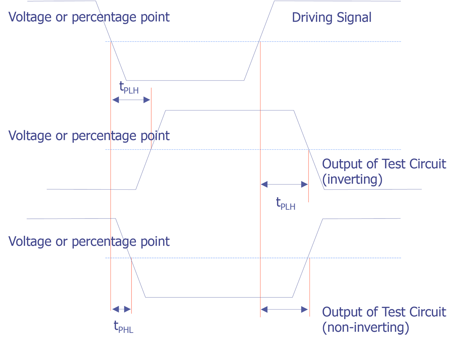
- Propagation delay time (tPHL). The time measured with the specified output changing from the defined HIGH level to the defined LOW level with respect to the corresponding input transition.
- Propagation delay time (tPLH). The time measured with the specified output changing from the defined LOW level to the defined HIGH level with respect to the corresponding input transition.
- APPARATUS. Equipment capable of measuring elapsed time between the input signal and output signal at any percentage point or voltage point between the maximum LOW level and minimum HIGH level shall be provided. The input shall be supplied by a driving source as described in Method 3001 of this standard. It is desirable for this equipment to have data logging capability so that circuit dynamic performance can be monitored. The test chamber shall be capable of maintaining the device under test at any specified temperature.
- PROCEDURE. The test circuit shall be loaded according to Method 3002 of this standard. The driving signal to the test circuit shall be provided according to Method 3001 of this standard. The device shall be stabilized at the specified test temperature.
- Measurements at a voltage point. tPLH and tPHL shall be measured from the threshold voltage point on the driving signal to the threshold voltage point on the test circuit output signal for both inverting and non-inverting logic. These delays shall be measured at the input and output terminals of the device under test. The device under test shall be conditioned according to the applicable procurement document with nominal bias voltages applied. Figure 3003-1 and Figure 3003-2 show typical delay measurements.
- Measurements at percentage points. tPLH and tPHL shall be measured from a specified percentage point on the driving signal to a specified percentage point on the test circuit output signal for both inverting and noninverting logic. These delays shall be measured at the input and output terminals of the device under test. The device under test shall be conditioned according to the applicable procurement document with nominal bias voltages applied. Figure 3003-1 and Figure 3003-2 show typical delay measurements.
- SUMMARY. The following details shall be specified in the applicable procurement document:
- tPLH and tPHL limits.
- Parameters of the driving signal: tTHL, tTLH, High Level, Low Level, Pulse Width, repetition rate.
- Load conditions.
- Conditioning voltages (static or dynamic).
- Measurement points (see 3.1 and 3.2).
- Power supply voltages.
- Test temperature.
MIL STD Procedures for Transition Time Measurements
MIL-STD-883C
METHOD 3004.1
TRANSITION TIME MEASUREMENTS
- PURPOSE. This method establishes the means for measuring the output transition times of digital microelectronic devices, such as TTL, DTL, RTL, ECL and MOS.
- Definitions. The following definitions shall apply for the purpose of this method.
- Rise time (tTLH). The transition time of the output from 10 percent to 90 percent or voltage levels of output voltage with the specified output changing from the defined LOW level to the defined HIGH level.
- Fall time (tTHL). The transition time of the output from 90 percent to 10 percent or voltage levels of output voltage with the specified output changing from the defined HIGH level to the defined LOW level.
- APPARATUS. Equipment capable of measuring the elapsed time between specified percentage points (normally 10 percent to 90 percent on the positive transition and 90 percent to 10 percent on the negative transition) or voltage levels. The test chamber shall be capable of maintaining the device under test at any specified temperature.
- PROCEDURE. The device shall be stabilized at the specified test temperature. The device under test shall be loaded as specified in the applicable procurement document. The load shall meet the requirements specified in Method 3002 of this document. The driving signal shall be applied as specified in Method 3001 or the applicable procurement document.
- Measurement of tTLH and tTHL. Unless otherwise stated, the rise transition time (tTLH) shall be measured between the 10 percent and 90 percent points on the positive transition of the output pulse and the fall transition time (tTHL) shall be measured between the 90 percent and 10 percent points on the negative transition of the output pulse. The device under test shall be conditioned according to the applicable procurement document with nominal bias voltages applied. Figure 3004-1 shows typical transition time measurement.
- SUMMARY. The following details shall be specified in the applicable procurement document:
- tTLH limits.
- tTHL limits.
- Transition time measurement points if other than 10% or 90%.
- Parameters of the driving signal.
- Conditioning Voltages (static or dynamic).
- Load condition.
- Power supply voltages.
- Test temperature.
MIL STD Procedures for Functional Testing
MIL-STD-883C
METHOD 3014
FUNCTIONAL TESTING
- PURPOSE. This method establishes the means for assuring circuit performance in regard to the test requirements necessary to verify the specified function and to assure that all logic element paths are not open, stuck-at-HIGH level or stuck-at-LOW LEVEL. This method applies to digital microelectronic devices, such as TTL, DTL, RTL, ECL and MOS.
- APPARATUS. An instrument shall be provided which has the capability of applying logic patterns (sequentially, if specified) to the logic network input(s), in accordance with the applicable procurement document. The test instrument shall also be capable of applying nominal power supply voltages and monitoring the outputs for the specified logic levels. The output monitoring circuit may be either a single or double comparator type. The threshold voltage (trip point) for a single comparator or VOL (max) and VOH (min) for a double comparator shall be specified in the applicable procurement document. The test chamber shall be capable of maintaining the device under test at any specified test temperature.
- PROCEDURE. The device shall be stabilized at the specified test temperature. Nominal power supply voltages and the specified input logic patterns shall be applied to the logic network under test and the output(s) monitored.
- SUMMARY. The following details shall be specified in the applicable procurement document:
- Test temperature.
- Power supply voltage.
- Input voltage levels.
- Input and output logic patterns.
- Output threshold voltage (see 2).
- VOH (min) and VOL (max) (see 2).
References on Electrical Test
- M. Abramovici, M. Breuer, and A. Friedman, Digital Systems Testing and Testable Design, Computer Science Press, 1990.
- A. Van de Goor, Testing Semiconductor Memories, theory and practice, John Wiley and Sons, 1991.
- R. Bennetts, Design of Testable Logic Circuits, Addison-Wesley Publishers, Limited, 1984.
- J. Cortner, Digital Test Engineering, John Wiley & Sons, Inc., 1987.
- J. Bateson, In-Circuit Testing, Van Nostrand Reinhold Company, Inc., 1985.
- C. Timoc, Selected Reprints on Logic Design for Testability, IEEE Computer Society Press, 1984.
- W. Needham, Designer's Guide to Testable ASIC Devices, Van Nostrand Reinhold Company, Inc., 1991.
- R. Rajsuman, Digital Harware Testing: Transistor-Level Fault Modeling and Testing, Artech House, Inc., 1992.
- M. Breuer and A. Friedman, Diagnosis and Reliability of Digital Systems, Computer Science Press, Inc., 1976.
- R. Gulati and C. Hawkins, IDDQ Testing of VLSI Circuits, Kluwer Academic Publishers, 1993.
- Books on basic electrical design and test principles, such as Introduction to VLSI Systems by Mead and Conway, Principles of CMOS VLSI Design by Weste and Eshraghian, and VLSI Design Techniques for Analog and Digital Circuits by Geiger, Allen, and Strader.
- Technical articles on basic electrical analysis techniques in the proceedings, tutorials, and workshops of the International Test Conference, International Symposium for Testing and Failure Analysis, and International Reliability Physics Symposium.