System Maintenance occurs every Friday.
System Maintenance occurs every Friday.
Fault localization is the process of tracing back signals through an integrated circuit to locate the first failing node. This process can be performed using either mechanical probing or electron beam probing. The task of fault localization is heavily dependent on the design of the IC and usually requires individuals knowledgeable about the design of the IC and the test patterns needed to stimulate the IC. Although some tools, such as Schlumberger's Diagnostic Assistant, exist to help automate this process, fault localization is usually a manual task with highly complex ICs.
Proper design and test considerations up front can help reduce the complexity of this task. Techniques such as scan design, IDDQ testing, and structured design and test principles can eliminate many hours of fault isolation later on during design validation and qualification.
Fault localization is necessary to determine the location of the defect. In most cases, the location of the defect is necessary to determine the root cause of failure. It is worth noting, however, that fault localization may not be necessary to give a satisfactory response to the requester. Many times, the requester is satisfied with a determination as to whether the defect is a wafer fabrication problem, a packaging problem, a testing problem, or an end use problem such as EOS/ESD.
Once the IC has been characterized electrically and the packaging material has been removed, the signal should be traced from the failing node back into the IC. At some point, gate causing the incorrect output can be found. While this sounds simple, with the complexity of modern ICs and the high fan outs found on many nodes, this process can get very tedious very quickly. Other non-contact methods, such as voltage contrast, are better suited to handle complicated ICs, but if they are not available, mechanical signal tracing is a very inexpensive alternative.
After the IC is placed in the failing electrical state and contact can be made to the metal or poly layer of interest, the rest is easy. Start from the failing output and trace the signals backward until a node is found in the wrong state. A common way to determine if a node is in the wrong state is to probe the same node on a comparison IC that is in the same electrical state. If possible, placing the two ICs side by side under the same probe station will help facilitate this process. Care must be taken at all times not to damage the IC with the probes.
The most cumbersome part of this process is dealing with complicated branching that takes place on many circuits. Remember that these ICs were not laid out for ease of signal tracing for failure analysis.
SN746 failed functional testing with the following pattern. Data at locations (addresses) 0, 192, 256, 704, 768, 1216, 1280, etc. were failing when checkboard, inverse checkboard, and unique address patterns were written and then read. The failures occurred across all eight bits of the data byte in a random fashion. The failure mode indicated that incorrect data were being read from the IC, suggesting a possible problem with addressing.
After exhausting the rapid localization techniques, we then moved to the electron beam probe to begin troubleshooting the three ICs. AN ATE provided stimulus to the IC in the electron beam probe. The diagram below, which describes the physical layout of the memory array, facilitates the following discussion (see Figure 1). The EEPROM uses X and Y decode signals to select rows. The X decode is a set of eight signals based on the values of address lines 6 through 8. The eight Y decode signals are based on the values of address lines 9 through 11. For example, if A8-6 has the value 011, then the X3 signal is high or active, if A8-6 has the value 101, then the X5 signal is active, and so on. The Y signals work in the same fashion as the X signals.
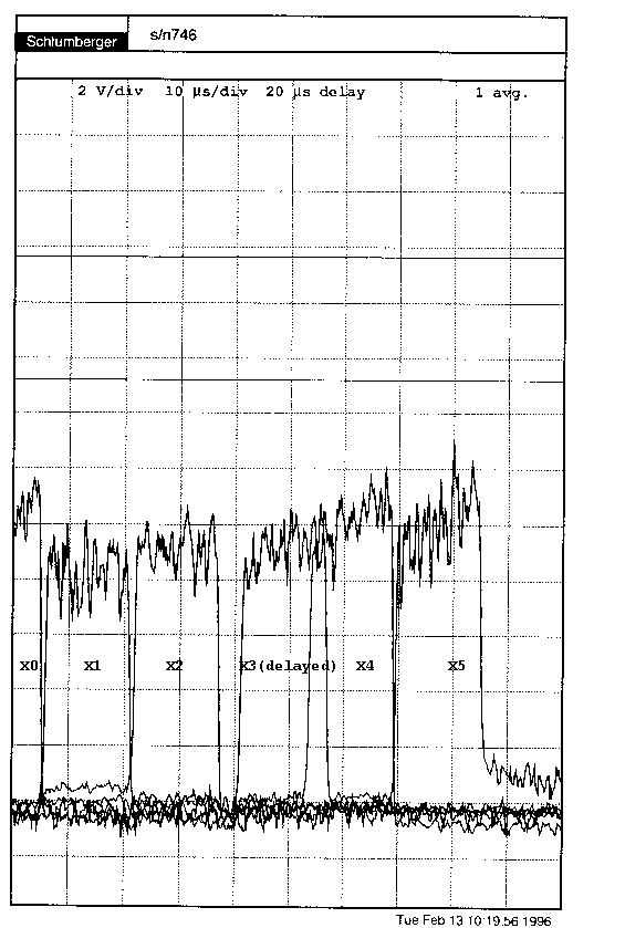
The failure on SN746 (0, 192, 256, 704, 768, etc.) produces the following binary sequence. This corresponds to the address lines of interest, which are A6-A8 (X decode signals). In particular, when the X group of addresses switches from X2 to X3 or from X3 to X4, the data on the first address is incorrect. This would indicate a delay on signal line X3. When signal line X3 was examined in the electron beam probe, a delay was observed after a particular metal 1 - metal 2 contact just before the signal line goes out to the memory array (see Figure 2).
| Y | X | ||||||||||||
|---|---|---|---|---|---|---|---|---|---|---|---|---|---|
| Addresses | A12 | A11 | A10 | A09 | A08 | A07 | A06 | A05 | A04 | A03 | A02 | A01 | A00 |
| 0 | 0 | 0 | 0 | 0 | 0 | 0 | 0 | 0 | 0 | 0 | 0 | 0 | 0 |
| 192 | 0 | 0 | 0 | 0 | 0 | 1 | 1 | 0 | 0 | 0 | 0 | 0 | 0 |
| 256 | 0 | 0 | 0 | 0 | 1 | 0 | 0 | 0 | 0 | 0 | 0 | 0 | 0 |
| 704 | 0 | 0 | 0 | 1 | 0 | 1 | 1 | 0 | 0 | 0 | 0 | 0 | 0 |
| 768 | 0 | 0 | 0 | 1 | 1 | 0 | 0 | 0 | 0 | 0 | 0 | 0 | 0 |
| 1216 | 0 | 0 | 1 | 0 | 0 | 1 | 1 | 0 | 0 | 0 | 0 | 0 | 0 |
Fault localization is performed usually after faster isolation techniques have been tried. You should first utilize techniques such as light emission, liquid crystal, fluorescent microthermographic imaging, CIVA, and LIVA before performing fault localization. In addition, before setting up for a manual fault isolation effort, check to see if there are any scan or IDDQ based techniques you can first try.
Fault localization using an e-beam probe should be performed before the top glass layer is removed. Fault localization using mechanical probes should be performed after the top glass layer is removed.
