System Maintenance occurs every Friday.

Transmission Electron Microscopy

Are you looking for more information regarding this and other subjects? Look no further than Semitracks' Online Training. Semitracks' Online Training contains short courses and other material useful for any Engineer trying to learn new subjects or brush up on old ones.

What is Transmission Electron Microscopy?

Overview

A TEM (transmission electron microscope) uses a highly energetic electron beam (100 keV - 1 MeV) to image and obtain structural information from thin film samples. The electron microscope consists of an electron gun, or source, and an assembly of magnetic lenses for focusing the electron beam. Apertures are used to select among imaging modes and to select features of interest for electron diffraction work. The sample is illuminated with an almost parallel electron beam, which is scattered by the sample. In crystalline materials, the scattering takes the form of one or more Bragg diffracted beams, which are used to form a transmission diffraction pattern. These diffraction patterns can be used to identify unknown phases in the sample. A bright-field image of the sample can be formed by looking at the straight-through, non-diffracted beam. Features in the sample that cause scattering have darker contrast in a bright-field image than those that cause little or no scattering. An electron diffraction pattern can be generated from a particular area in a bright-field image (such as a particle or grain) by using a selected area aperture. Dark-field images are formed from a single diffracted beam and are used to identify all the areas of a particular phase having the same crystalline orientation. Magnifications from about 100x up to several hundred thousand times can be achieved in the TEM.

History

After the theory of the wave nature of electrons was developed by Louis DeBroglie in 1925, researchers Knoll and Ruska proposed the idea of an electron microscope. In 1936, the first electron microscope was built by Metropolitan-Vickers in the U.K. After World War II, several manufacturers, including Hitachi, JEOL, Philips, and RCA began manufacturing electron microscopes. In the late 1940's, Heidenreich first thinned specimens to electron transparency. Hirsh and his colleagues at Cambridge then developed the theory of electron diffraction contrast and documented his work in a large volume sometimes referred to as the "TEM Bible." The use of TEM for materials science work and semiconductor analysis has increased rapidly in the past two decades. This trend is likely to continue as feature sizes shrink. The TEM is probably one of the best positioned tools for examination of semiconductor structures for the foreseeable future.

TEM Basics

Electron Optics

There are basically three types of electron guns on today's transmission electron microscopes: 1. the tungsten cathode, 2. the lanthanum hexaboride (LaB6) cathode, and 3. the field emission gun. The three electron guns are described briefly below.

1. Tungsten cathode

The tungsten cathode is a fine wire approximately 100mm in diameter that has been bent into the shape of a hairpin with a V-shaped tip. The tip is heated to around 2400°C by passing current through it. At this temperature, one can expect a current density of approximately 1.75 A/cm2. The electrons will have a potential distribution of 0 to 2 volts. With a bias voltage between 0 and 500 volts, the electrons can be accelerated toward the anode. At an emission of 1.75 A/cm2, the lifetime of the tungsten filament is approximately 50 hours. A schematic diagram of a tungsten cathode is shown below (see Figure 1).

Schematic of a tungsten filament (self-biased) electron gun (after Goldstein et. al.). Schematic of a tungsten filament (self-biased) electron gun (after Goldstein et. al.).
Schematic of a tungsten filament (self-biased) electron gun (after Goldstein et. al.).

2. Lanthanum hexaboride (LaB6) cathode

As the need for higher resolution imaging increased, so did the need for brighter filaments. The most straightforward method to achieve this goal is to find a material with a lower work function Ew. A lower work function means more electrons at a given temperature, hence a brighter filament and higher resolution. Lathanum hexaboride, commonly known as LaB6, has been the best material developed to date for this application. The LaB6 filament operates at approximately 2125°C, resulting in a brightness on the order of five times brighter than a tungsten filament under the same conditions. LaB6 filaments tend to be an order of magnitude more expensive than tungsten filaments. A schematic of the LaB6 filament is shown in Figure 2.

Gun configuration for a LaB6 cathode (after Goldstein et. al.). Gun configuration for a LaB6 cathode (after Goldstein et. al.).
Gun configuration for a LaB6 cathode (after Goldstein et. al.).

3. Field Emission Gun

Another method for generating electrons is the field emission gun. When the cathode forms a very sharp tip (typically 100 nm or less) and the cathode is placed at a negative potential with respect to the anode, so that the local field at the tip is very strong (greater than 107 V/cm), electrons can tunnel through the potential barrier and become free. Although the total current is lower than either the tungsten or the LaB6 emitters, the current density is between 103 and 106 A/cm, making it hundreds of times brighter than a thermionic emission source. Furthermore, since the electrons are field-generated rather than thermally generated, the tip remains at room temperature. Tips are usually made from tungsten, etched in the <111> plane to generate the lowest work function. Because a native oxide will quickly form on the tip even at moderate vacuum levels (10 mPa), a high vacuum system (10 nPa) is needed. To keep the tip diameter sufficiently small, the cathode can be kept warm (800-1000 °C ) or rapidly heated to approximately 2000F °C for a few seconds to blow off material. A schematic of a field emission tip is shown in Figure 3.

Gun configuration for field emission (after Goldstein et. al.). Gun configuration for field emission (after Goldstein et. al.).
Gun configuration for field emission (after Goldstein et. al.).

Electron Lenses

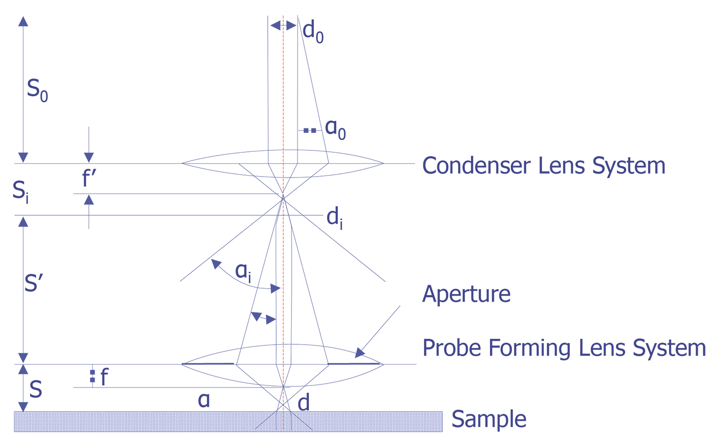
The electron beam is focused using electromagnetic lenses. The condenser lens system, which is composed of one or more lenses, determines the beam current that impinges on the sample. The probe-forming lens, often called the objective lens, determines the final spot size of the electron beam. Conventional electromagnetic lenses are used and the electron beam is focused by the interaction of the electromagnetic field of the lens on the moving electrons. A schematic depiction of the scanning electron microscope column is shown below (see Figure 4). The a angles drawn in Figure 4 are exaggerated on purpose to more clearly show the effect of the lenses on the electron optics. The probe lens can be adjusted to focus the beam depending on the working distance.

The working distance is defined as the distance between the bottom pole piece of the objective lens and the sample surface. It is typically 5 to 25 mm. As the working distance is increased, the spot size increases on the sample, given the same final aperture lens. There is a second tradeoff between spot size and beam current. The spot size is directly controlled by minimizing di (see Figure 4). However, by minimizing di, the beam current falls off by the ratio (aa/ai)2. The operator must make a conscious decision as to whether the analysis requires minimizing the beam spot size or maximizing the beam current.

Schematic of ray traces in a typical scanning electron microscope column (after Goldstein et. al.). Schematic of ray traces in a typical scanning electron microscope column (after Goldstein et. al.).
Schematic of ray traces in a typical scanning electron microscope column (after Goldstein et. al.).

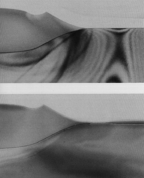
Several aberrations can occur in an electron optical column. These include: spherical aberration, chromatic aberration, diffraction, and astigmatism. The first three are depicted schematically in Figure 5. Spherical aberration results from non-uniformity of the lenses. Electrons which pass through the lens further off the optical axis are pulled more strongly than those that pass through near the center of the lens. To reduce this effect, the final aperture can be reduced, but this results in a lower beam current.

Chromatic aberration results from differences in electron velocity through the lenses. Electrons with higher velocity or energy will be bent more strongly by the magnetic lenses, resulting in a dull or blurred image. Other than more expensive LaB6 or field emission instruments, no other techniques exist to address this problem. Tungsten filament systems typically have a 2 eV spread when leaving the cathode; LaB6 systems have a 1 eV spread, and field emission systems have a 0.2 to 0.5 eV spread. Diffraction occurs because of the wave nature of electrons and the aperture size of the final lens. The only way to reduce diffraction problems is to increase the final aperture size. Astigmatism results from the fact that magnetic lenses do not have perfect symmetry. Machining errors can cause lens systems to be slightly elliptical, rather than perfectly circular, and irregularities in the iron windings can cause variations in the magnetic field. Most instruments contain a stigmator in the final lens system to help compensate for this effect. The stigmator usually has two controls, one to correct for the magnitude of the asymmetry and one to correct for the direction of the asymmetry of the main field. The stigmator can only correct for asymmetry in the final lens. It cannot correct dirty aperture or filament misalignment.

Schematic drawings showing spherical and chromatic aberrations as well as diffraction at a lens aperture (adapted from Hall, Oatley, and Goldstein et. al.). Schematic drawings showing spherical and chromatic aberrations as well as diffraction at a lens aperture (adapted from Hall, Oatley, and Goldstein et. al.).
Schematic drawings showing spherical and chromatic aberrations as well as diffraction at a lens aperture (adapted from Hall, Oatley, and Goldstein et. al.).

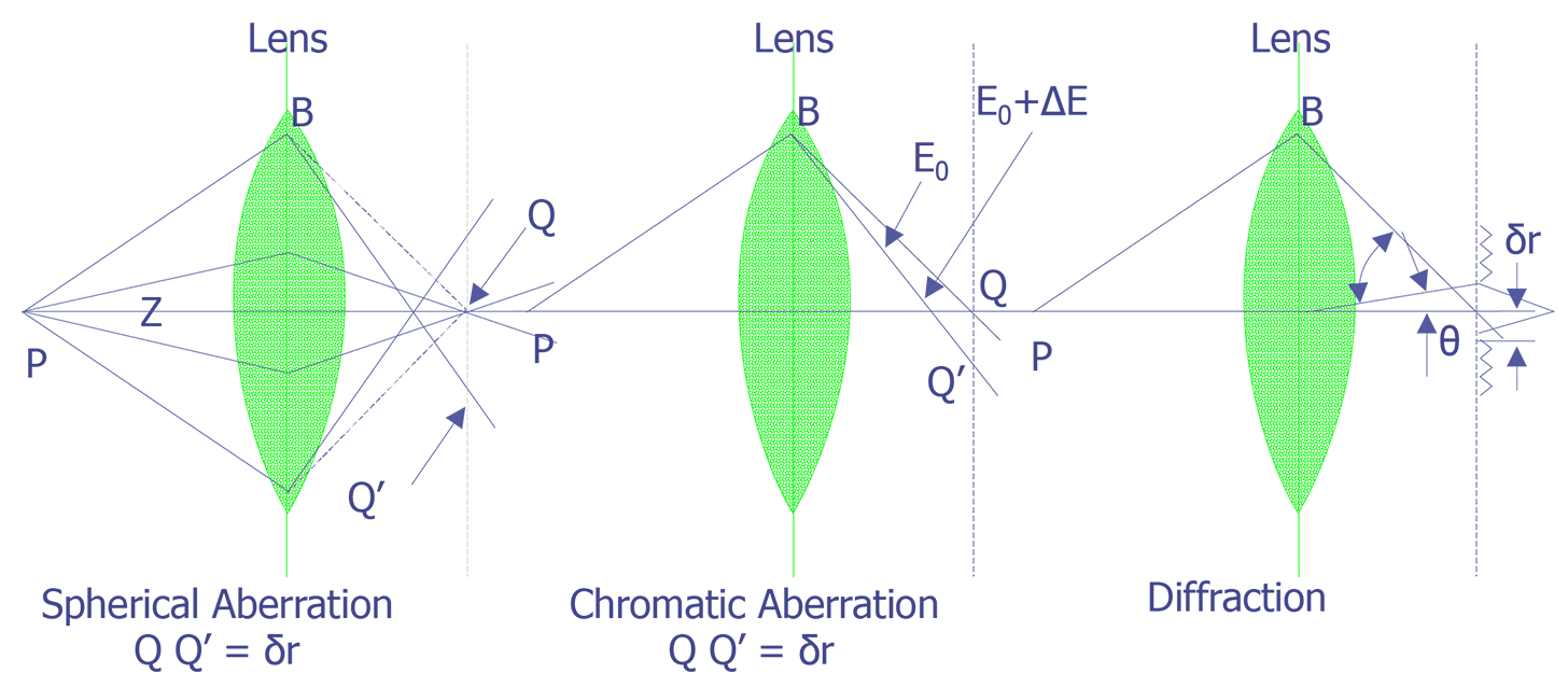
Figure 6 shows the relationship between probe current and beam diameter for both tungsten and LaB6 systems. These values were taken with the tungsten gun current density at 4.1 A/cm2 and the LaB6 gun current density at 25 A/cm2.

Relationship between probe current and the size of the electron beam. Calculations use the W hairpin filament and the LaB6 gun operating at 15 and 30 kV (after Goldstein et. al.). Relationship between probe current and the size of the electron beam. Calculations use the W hairpin filament and the LaB6 gun operating at 15 and 30 kV (after Goldstein et. al.).
Relationship between probe current and the size of the electron beam. Calculations use the W hairpin filament and the LaB6 gun operating at 15 and 30 kV (after Goldstein et. al.).

Why Perform Transmission Electron Microscopy?

There are several basic reasons for using a transmission electron microscope: resolution, depth of field, ability to identify elements, and ability to determine crystalline structure.

Resolution

According to classical Rayleigh criteria, the smallest distance that can be resolved, δ, is given approximately by

The smallest distance that can be resolved, delta, is given by this equation. The smallest distance that can be resolved, delta, is given by this equation.

where λ is the wavelength of the radiation, μ is the refractive index of the viewing medium, and β is the semiangle of collection of the magnifying lens. DeBroglie's equation shows that the wavelength λ of electrons is related to their energy, E, by the following equation

This equation shows that the wavelength lambda of electrons is related to their energy. This equation shows that the wavelength lambda of electrons is related to their energy.

Based on these two equations, a TEM imaging a sample with 100 keV electrons is capable of a theoretical resolution of 0.004 nm (much smaller than the diameter of an atom). In reality, this resolution is not achieved because of our inability to make a "perfect" electron lens. However, the resolution of the TEM is far greater than that of an optical microscope, which is approximately 300 nm for a microscope using visible wavelengths of light.

Depth of Field

Because of the intensity of the electron source, we can place a small aperture in front of an electron source, we can dramatically increase the depth of field. A light microscope must have a large aperture in order to capture enough light to make an image. This in turn creates a very small depth of field.

Ability to Identify Elements and Crystalline Structure

Because the electron beam interacts with elements in the specimen, we can obtain information on the specimen based on signals generated from the interaction. For example, we can use the characteristic x-rays generated to perform energy dispersive x-ray analysis, or use the energy from the inelastically scattered electrons to perform electron energy-loss spectrometry (EELS). We can also use information from elastically scattered electrons to create electron diffraction patterns that can yield data as to the crystalline structure of the specimen.

Even though the transmission electron microscope has several advantages over other instruments, there are a number of factors that make the technique more difficult to use. These include: expertise, expense of the instrument, and sample preparation.

Expertise

Although the operation of modern transmission electron microscopes is fairly straightforward, the interpretation of the images and spectrometry data requires expertise. Typically, a combination of education in physics and experience in interpreting TEM data is necessary. Many companies may employ a TEM expert. In any case, it is necessary to have a full-time operator.

Expense of the Instrument

Transmission Electron Microscopes are relatively expensive instruments. New systems currently cost between $500k and $1M (U.S.). This is more than standard scanning electron microscopes and considerably more than optical microscope systems.

Sample Preparation

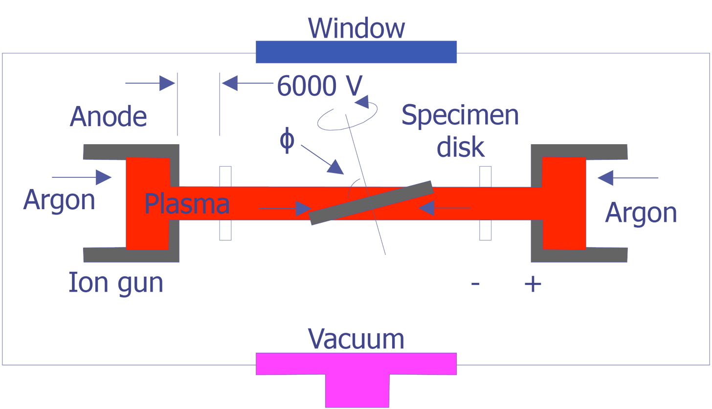
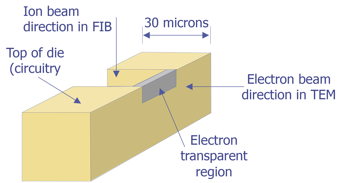
TEM sample preparation is still very much an art. The ability to polish a specimen to electron transparency evenly over several tens of microns takes a good deal of practice and patience. The advent of the focused ion beam is making TEM sample preparation easier, but a focused ion beam system is a very expensive instrument to be routinely used for this purpose.

Uses for the Transmission Electron Microscope

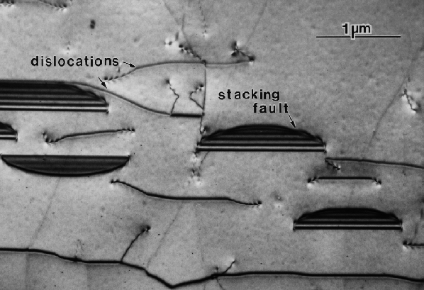
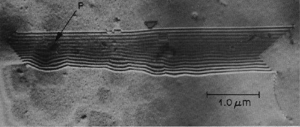
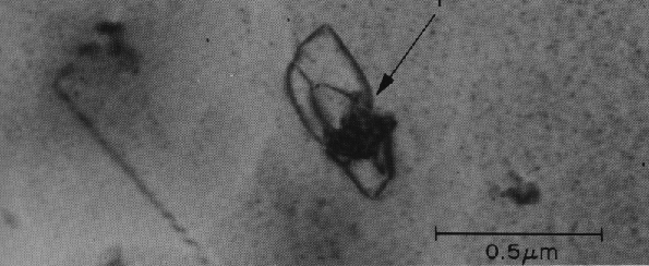
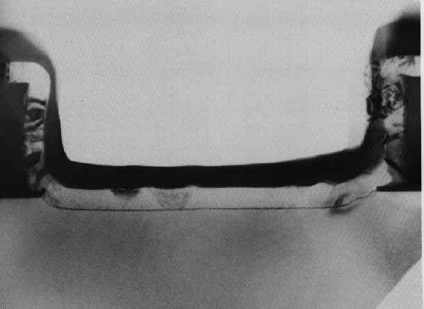
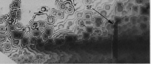
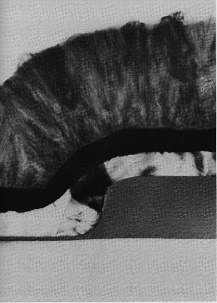
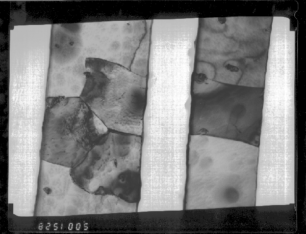
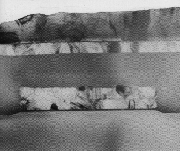
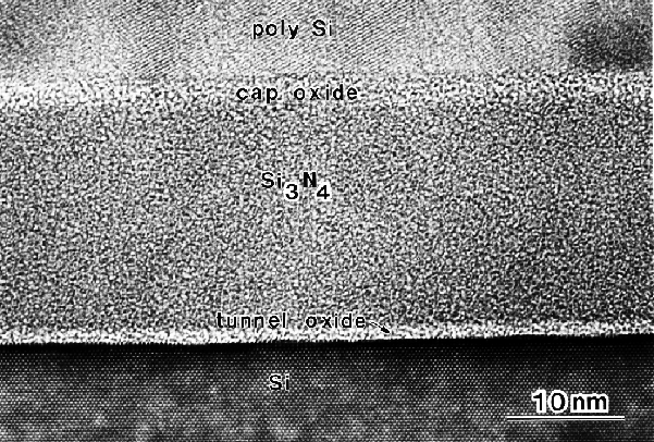
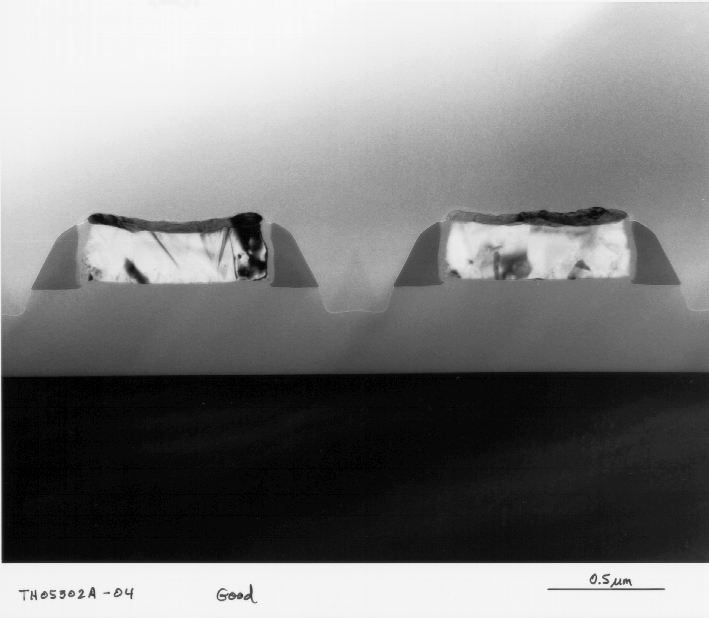
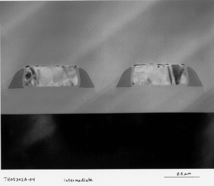
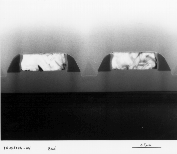
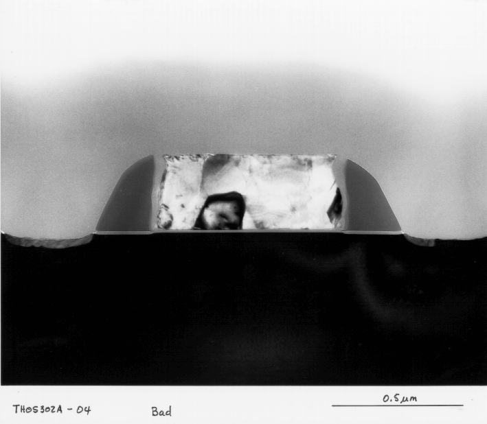
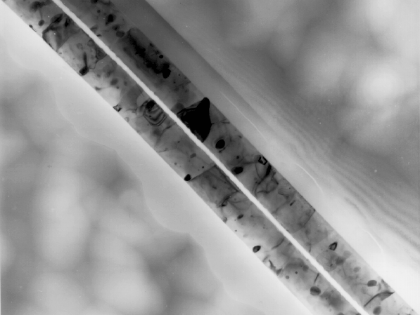
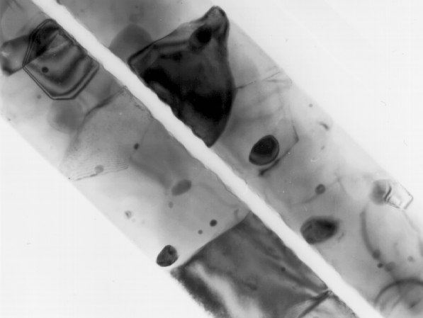
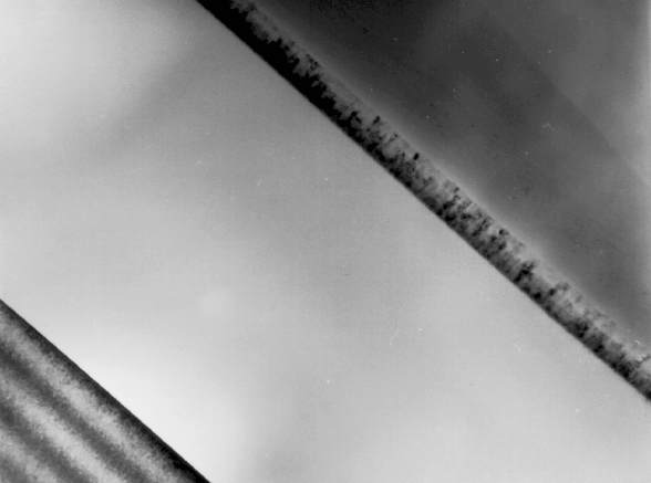
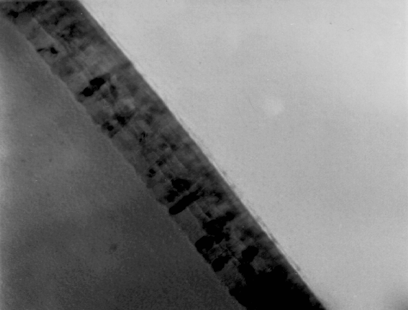
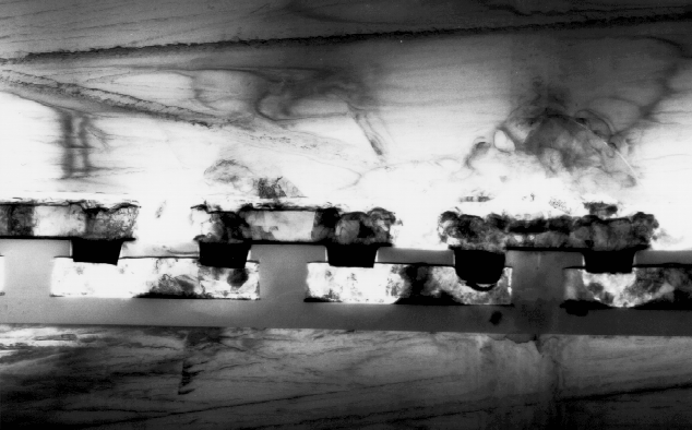
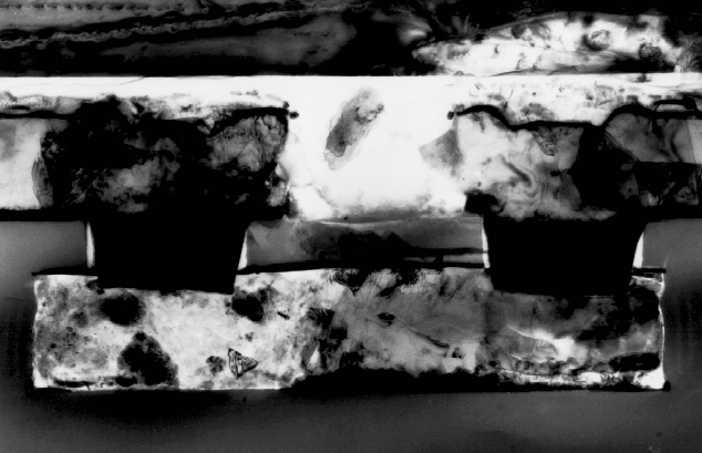
A TEM is used to obtain structural information about a sample. TEM imaging is used routinely to examine thinned cross-sections of ICs and electronic devices to observe metal and polysilicon grain structure, crystalline defects in silicon (such as stacking faults and dislocations), diffusion barriers, thin metallization layers, defects in gate oxide layers, etc. TEM examination can reveal layer thicknesses and step coverage, show implanted regions, and provide delineation of p/n junctions. Because TEM sample preparation is fairly laborious, TEM analysis is generally reserved for solving those problems that can't be handled with other tools, such as the SEM.

When is Transmission Electron Microscopy Performed?

Because TEM sample preparation is destructive, TEM analysis should be performed only after all other analyses have been performed on an IC. Some of the information obtained from TEM analysis can also be obtained from SEM examination of focused ion beam (FIB) or mechanically cross-sectioned devices. These alternative methods should be used whenever possible because of the comparative ease of sample preparation.

How is Transmission Electron Microscopy Performed?

Transmission electron microscopes are complex pieces of equipment, and proper training is required in order to operate one. Unless you are a skilled TEM operator yourself, a TEM expert should perform this analysis for you. Your role will be to communicate to the operator what information you need to acquire from the sample, what areas need to be examined, and the like.

Standard TEM sample preparation procedure

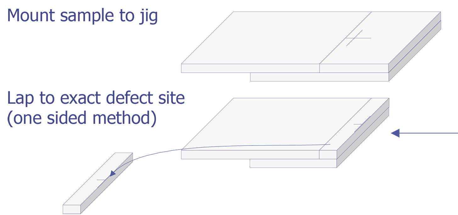
TEM sample preparation for most integrated circuit applications is a two-step procedure that first involves polishing and then ion milling. To prepare a sample for TEM imaging, use the following procedure:

  1. Cut the sample into several strips such that there are multiple opportunities to image the feature of interest (see Figure 7). For example, if you wish to image a transistor cross section, cut the IC into pieces along the axis where multiple transistor cross sections will be present. This will increase your odds of obtaining a useful sample the first time.
    Sequence of steps for preparing the sandwich structure during TEM sample preparation. Sequence of steps for preparing the sandwich structure during TEM sample preparation.
    Sequence of steps for preparing the sandwich structure during TEM sample preparation.
  2. Arrange the strips in between two glass or silicon strips and create a sandwich structure. Glue the sandwich structure to the TEM grid (see Figure 7).
  3. Using the appropriate polishing equipment, polish the sample to a thickness of less than 2 microns. A thickness of less than 1 micron is even better. The best technique for this is to use a tripod polisher. Use a very flat polishing wheel, such as a glass platen. Use a micrometer to level the tripod. Use diamond lapping films that do not have adhesive backing and be sure to use a new cloth for each sample to be prepared. To minimize the effect of debris, be sure to orient the interfaces in the cross section samples normal to the radius of the wheel. Also, be sure to not cross the debris trail during polishing.
  4. Next, use ion milling to thin the sample to electron transparency. Place your sample in the ion mill with the surface of the specimen at an angle of 15-25° to the surface (see Figure 8). Sometimes, a much lower angle of incidence (£ 5°) can be used to avoid preferential etching. Because the reduced angle can lead to increased damage near the surface, it is often necessary to lower the beam energy to reduce damage. This obviously increases the milling time. Normally, the specimen should be rotated and cooled during milling. Rotation tends to reduce surface structures caused by the milling, while cooling tends to reduce atom migration in the specimen.
    Schematic diagram of an ion beam thinning device. The system is under vacuum and can be placed at liquid nitrogen temperature. Schematic diagram of an ion beam thinning device. The system is under vacuum and can be placed at liquid nitrogen temperature.
    Schematic diagram of an ion beam thinning device. The system is under vacuum and can be placed at liquid nitrogen temperature.

Procedure for preparing TEM samples using a Focused Ion Beam System

This method is most useful if you need to image a particular point defect, because it yields the best chance for imaging the defect.

  1. Prepare the device to be sectioned by doing any preliminary deprocessing. Sometimes it is helpful to remove top layers of the IC in order to better expose the region of interest, if it is buried deep in the process. An example of this would be examining a gate oxide defect by removing some or all of the metal layers above the defect.
  2. Place fiduciary marks to highlight the area of interest if possible. This is best accomplished with a laser cutter. You may want to etch a cross or gun sight mark to highlight the area of interest. Be sure to use the smallest aperture when close to the region of interest. This cross pattern should allow you to see the region of the defect with the naked eye. You may also want to make a mark to designate the direction in which the IC is to be lapped. This is useful on ICs with regular structure, such as memory ICs.
  3. Mount the sample to the polishing stub with a thermal wax (see Figure 9). For the one-sided method, it should be mounted opposite the orientation expected for an SEM cross section. Later, it will be reversed for a final polish to the area of interest. The failing area should not overhang the stub by too much so as to lessen the chance of breaking (as in the normal SEM preparation). Care should be taken to align the die to the required angle before the wax sets.
    Graphical representation of necessary steps to prepare a sample for TEM imaging using a Focused Ion Beam (FIB) system (after Morris et. al.). Graphical representation of necessary steps to prepare a sample for TEM imaging using a Focused Ion Beam (FIB) system (after Morris et. al.).
    Graphical representation of necessary steps to prepare a sample for TEM imaging using a Focused Ion Beam (FIB) system (after Morris et. al.).
  4. Attach the stub to the polishing fixture and lap away the excess portion of the die. Start with a course grit disc at first and use progressively finer grit discs until you are within 40 - 50 microns of the failing area. At that point, switch to a glass wheel and lap with flowing water for the remainder of the polish. Lap to within 30 microns of the failure for the one-sided method and to within 15 microns for the two-sided method. Do not go any closer. Be sure to examine the sample often during this procedure to monitor your progress. Making the sample as smooth as possible will reduce the possibility of fracturing the sample.
  5. Remove the stub from the polishing fixture. Heat the stub until the wax is soft and remove the sample from the stub. The remaining wax can be removed with acetone. An ultrasonic bath can be used as a final clean at this point.
  6. Make a silicon jig (see Figure 10). This can be made with two dice you do not intend to use. Use two dice with the same area and thickness. Glue two of these dummy dice back to back with a 50% overhang. Cyanacrylate adhesive (superglue) makes a good adhesive. Be sure to use only a small amount so that excess glue does not appear from the interface.
    Graphical representation of necessary steps to prepare a sample for TEM imaging using a Focused Ion Beam (FIB) system (after Morris et. al.). Graphical representation of necessary steps to prepare a sample for TEM imaging using a Focused Ion Beam (FIB) system (after Morris et. al.).
    Graphical representation of necessary steps to prepare a sample for TEM imaging using a Focused Ion Beam (FIB) system (after Morris et. al.).
  7. Heat the stub and mount the silicon jig to it using thermal wax. The easiest way to do this is by placing a few flakes of wax on the exposed area of the overhanging silicon while it is on the hot plate. Under a low power microscope while the wax is still supple, orient the sample parallel to the original lapped surface and completely off the stub. Let the sample cool and remove any excess wax with acetone.
  8. Reattach the stub to the polishing fixture and remove the excess silicon in a manner similar to step four. If using the two-sided method, polish to within 15 microns of the region of interest; if using the one-sided method, polish to the region of interest. Be sure to check after every few seconds (2 - 5) on the polishing wheel once you are within 5 microns. When you are within 2 microns of the area of interest, examine the IC from the cross-sectional view to determine an appropriate stopping place. For a gate oxide defect, an appropriate stopping place would be the edge of the poly-silicon gate.
  9. Remove the stub from the polishing fixture. Heat the stub until the wax is soft enough to remove the jig containing the TEM sample from the stub. Place the jig in an acetone bath and let soak until the TEM sample falls away from the jig. You can aid the process by swishing the jig around in the solution. Once the sample is separated, let it soak a few minutes longer to remove all of the wax.
  10. Pour off the acetone, being sure to keep the TEM sample. One way to do this is to pour into a large glass Petri dish and blot up the acetone with a paper towel. This should leave the TEM sample alone in the Petri dish.
  11. Under a low power microscope, modify the three millimeter copper grid by cutting a pie shaped wedge out of it with a sharp scalpel (cut out a 60% arc).
  12. Trim away any excess length on the TEM sample so that it will not overhang the copper grid. Be sure to cover the sample with your hand so it doesn't fly away during the cutting process. You can also grind away the excess material earlier on in the grinding process while the sample is in a stronger mechanical condition.
  13. Using a pair of extremely fine point tweezers, pick up the sample and lay it across the grid so that the area of interest straddles the hole in the copper grid (see Figure 11). This step requires some patience and a steady hand, but can be accomplished relatively easily if the tweezers are sharp.
    Graphical representation of necessary steps to prepare a sample for TEM imaging using a Focused Ion Beam (FIB) system (after Morris et. al.). Graphical representation of necessary steps to prepare a sample for TEM imaging using a Focused Ion Beam (FIB) system (after Morris et. al.).
    Graphical representation of necessary steps to prepare a sample for TEM imaging using a Focused Ion Beam (FIB) system (after Morris et. al.).
  14. Pluck a bristle from a paint brush. Use this bristle to apply a very small drop of super glue to the copper grid just below the sample. Place the drop close enough so that the drop will spread out and contact the TEM sample. Immediately start sliding the copper grid around on top of the dish to prevent the grid from becoming attached to the dish. If you mess up, soak the copper grid in acetone and try this step again.
  15. Mount the copper grid end up onto an SEM type mounting stud (see Figure 12). Do this by placing a dab of thick silver epoxy on the stub and embedding the copper grid into the silver epoxy. Bake the stub containing the copper grid and sample at 100 degrees for a few minutes to harden the silver epoxy.
    Graphical representation of necessary steps to prepare a sample for TEM imaging using a Focused Ion Beam (FIB) system (after Morris et. al.). Graphical representation of necessary steps to prepare a sample for TEM imaging using a Focused Ion Beam (FIB) system (after Morris et. al.).
    Graphical representation of necessary steps to prepare a sample for TEM imaging using a Focused Ion Beam (FIB) system (after Morris et. al.).
  16. If you wish to decrease FIB milling times, you can blast the area of the TEM sample to be milled with a laser beam repeatedly to disrupt the silicon lattice. This has the effect of increasing the milling rate and decreasing the milling time. Be sure not to blast the area of interest, or you will damage the sample.
  17. If your FIB system does not have a charge neutralizer, coat the specimen to prevent beam drift. Drift of the beam could be disastrous during the final thinning cuts. However, you are better off not coating the sample if at all possible. Coating the sample will preclude any EDX work.
  18. Mount the stub in the FIB and power up the FIB. Make sure the beam is on long enough to reach stability.
  19. Locate the area of interest and zoom in. Switch to the largest aperture available. Define a milling area box that will remove material aligned with the specimen. Don't mill too close to the area of interest on the largest aperture. Mill to approximately 8 microns deep on a 30 micron TEM sample (see Figure 13 and Figure 14). This should be sufficient to allow a variety of tilt angles to be used when viewing the specimen. This box should result in a milling time of 90 minutes or less. Once the bulk cut is complete, mill smaller rectangles successively closer to the area of interest. Switch to progressively smaller apertures as necessary. Continue milling until the TEM window is approximately 1000 angstroms or less. Be sure to carefully align your milling box with the sample to produce a uniform thickness TEM window.
    Graphical representation of a TEM sample after using a Focused Ion Beam (FIB) system for sample preparation (after Morris et. al.). Graphical representation of a TEM sample after using a Focused Ion Beam (FIB) system for sample preparation (after Morris et. al.).
    Graphical representation of a TEM sample after using a Focused Ion Beam (FIB) system for sample preparation (after Morris et. al.).
    Grey areas represent the TEM sample FIB milled areas using the one-sided method (left) and the two-sided method (right) (after Morris et. al.). Grey areas represent the TEM sample FIB milled areas using the one-sided method (left) and the two-sided method (right) (after Morris et. al.).
    Grey areas represent the TEM sample FIB milled areas using the one-sided method (left) and the two-sided method (right) (after Morris et. al.).
  20. Remove the sample holder with the grid from the FIB. Carefully remove the grid using tweezers and mount the grid in the TEM. You are now ready to image the specimen.

Electron energy loss spectroscopy (EELS) is the analysis of the distribution of electron energies emergent from a thin-foil specimen. The electrons in the primary beam are decelerated and lose energy as they pass through the thin sample by several mechanisms, but it is the loss due to ionization of inner shell electrons in the sample that provides the most useful information. The electron spectrometers used for EELS detection are electrostatic or magnetic. The EELS technique is more sensitive to light elements than is EDS; hence, EDS and EELS are often used as complementary techniques.


References on TEM

  1. D. B. Williams and C. B. Carter, Transmission Electron Microscopy - A Textbook for Materials Science, Plenum Press, New York, 1996.
  2. J. A. Chandler, X-Ray Microanalysis in the Electron Microscope, North-Holland Publishing Co., Amsterdam, 1977.
  3. J. W. Edington, Practical Electron Microscopy in Materials Science, Van Nostrand Reinhold Co., New York, 1976.
  4. P. Hirsch, A. Howie, R. B. Nicholson, D. W. Pashley, and M. J. Whelan, Electron Microscopy of Thin Crystals, Robert E. Krieger Publishing Co., Malabar, FL, 1977.
  5. D. C. Joy, A. D. Romig, Jr., and J. I. Goldstein, Principles of Analytical Electron Microscopy, Plenum Press, New York, 1986.
  6. R. B. Marcus and T. T. Sheng, Transmission Electron Microscopy of Silicon VLSI Circuits and Structures, John Wiley & Sons, New York, 1983.
  7. A. D. Romig., Jr., "Analytical Transmission Electron Microscopy" (in Metals Handbook, 9th Edition, Vol. 10, R. E. Whan, coordinator, American Society for Metals, Metals Park, Ohio, 1986), pp. 429 - 453.
  8. T. T. Sheng, "Cross-Sectional Transmission Electron Microscopy of Electronic and Photonic Devices", contained in Analytical Techniques for Thin Films, (edited by K. N. Tu and R. Rosenberg, Academic Press Inc, 1988), pp. 251 - 296.
  9. D. B. Williams, Practical Analytical Electron Microscopy in Materials Science, Philips Electronic Instruments, Inc., Electron Optics Publishing Group, Mahwah, New Jersey, 1984.
  10. S. Morris, S. Tatti, E. Black, N. Dickson, H. Mendez, B. Schwiesow, and R. Pyle, A Technique for Preparing TEM Cross Sections to a Specific Area Using the FIB," Proc.Int. Symp. for Test. and Fail. Anal., Nov. 1991, pp. 417-427.
  11. A. W. Agar, R. H. Alderson, and D. Chescoe, Principles and Practice of Electron Microscope Operation, North-Holland Publishing Co., Amsterdam, 1974.
TEM cross section image showing a series of loops at the same depth in the silicon produced by ion implantation of source and drain regions of a transistor. (Courtesy Lucent Technologies). TEM cross section image showing a series of loops at the same depth in the silicon produced by ion implantation of source and drain regions of a transistor. (Courtesy Lucent Technologies).
Figure 1. TEM cross section image showing a series of loops at the same depth in the silicon produced by ion implantation of source and drain regions of a transistor. (Courtesy Lucent Technologies).
Plan-view image of oxidation-induced stacking faults and dislocations in a silicon substrate. (Courtesy Sandia National Laboratories). Plan-view image of oxidation-induced stacking faults and dislocations in a silicon substrate. (Courtesy Sandia National Laboratories).
Figure 2. Plan-view image of oxidation-induced stacking faults and dislocations in a silicon substrate. (Courtesy Sandia National Laboratories).
Plan view image showing both a stacking fault and a particle in the silicon substrate. These defects were associated with a light emitting defect in a p/n junction. The sample was prepared by thinning from the back side of the device. (Courtesy Lucent Technologies). Plan view image showing both a stacking fault and a particle in the silicon substrate. These defects were associated with a light emitting defect in a p/n junction. The sample was prepared by thinning from the back side of the device. (Courtesy Lucent Technologies).
Figure 3. Plan view image showing both a stacking fault and a particle in the silicon substrate. These defects were associated with a light emitting defect in a p/n junction. The sample was prepared by thinning from the back side of the device. (Courtesy Lucent Technologies).
Higher magnification image of the precipitate particle and the dislocations around it. (Courtesy Lucent Technologies). Higher magnification image of the precipitate particle and the dislocations around it. (Courtesy Lucent Technologies).
Figure 4. Higher magnification image of the precipitate particle and the dislocations around it. (Courtesy Lucent Technologies).
Cross-sectional image of a metal to silicon contact. The metal penetrates deeply into the silicon substrate, indicating that the substrate contacts were overetched. (Courtesy Lucent Technologies). Cross-sectional image of a metal to silicon contact. The metal penetrates deeply into the silicon substrate, indicating that the substrate contacts were overetched. (Courtesy Lucent Technologies).
Figure 5. Cross-sectional image of a metal to silicon contact. The metal penetrates deeply into the silicon substrate, indicating that the substrate contacts were overetched. (Courtesy Lucent Technologies).
Plan view image showing dislocations and stackings faults on a silicon substrate. (Courtesy Lucent Technologies). Plan view image showing dislocations and stackings faults on a silicon substrate. (Courtesy Lucent Technologies).
Figure 6. Plan view image showing dislocations and stackings faults on a silicon substrate. (Courtesy Lucent Technologies).
Cross-sectional image showing two examples of polysilicon grain structure. The lower layer of polysilicon in this device has relatively large grains, while the upper polysilicon layer is fine-grained. The microstructure of the polysilicon depends upon the deposition conditions and subsequent thermal cycles that the material experiences. (Courtesy Lucent Technologies). Cross-sectional image showing two examples of polysilicon grain structure. The lower layer of polysilicon in this device has relatively large grains, while the upper polysilicon layer is fine-grained. The microstructure of the polysilicon depends upon the deposition conditions and subsequent thermal cycles that the material experiences. (Courtesy Lucent Technologies).
Figure 7. Cross-sectional image showing two examples of polysilicon grain structure. The lower layer of polysilicon in this device has relatively large grains, while the upper polysilicon layer is fine-grained. The microstructure of the polysilicon depends upon the deposition conditions and subsequent thermal cycles that the material experiences. (Courtesy Lucent Technologies).
Plan view image showing the grain structure in patterned, sputter-deposited aluminum - 1% silicon metallization lines. The grain size is 2 - 4 micrometers. (Courtesy Allied Signal Kansas City Division). Plan view image showing the grain structure in patterned, sputter-deposited aluminum - 1% silicon metallization lines. The grain size is 2 - 4 micrometers. (Courtesy Allied Signal Kansas City Division).
Figure 8. Plan view image showing the grain structure in patterned, sputter-deposited aluminum - 1% silicon metallization lines. The grain size is 2 - 4 micrometers. (Courtesy Allied Signal Kansas City Division).
An example of a typical, defect-free gate oxide. The gate oxide is approximately 23 nanometers thick. (Courtesy Lucent Technologies). An example of a typical, defect-free gate oxide. The gate oxide is approximately 23 nanometers thick. (Courtesy Lucent Technologies).
Figure 9. An example of a typical, defect-free gate oxide. The gate oxide is approximately 23 nanometers thick. (Courtesy Lucent Technologies).
An example of a process-induced gate oxide thinning defect. Thin areas of a gate oxide are susceptible to failure by dielectric breakdown. (Courtesy Lucent Technologies). An example of a process-induced gate oxide thinning defect. Thin areas of a gate oxide are susceptible to failure by dielectric breakdown. (Courtesy Lucent Technologies).
Figure 10. An example of a process-induced gate oxide thinning defect. Thin areas of a gate oxide are susceptible to failure by dielectric breakdown. (Courtesy Lucent Technologies).
An example of a tunnel oxide in a non-volatile memory transistor. Tunnel oxides are very thin (approximately 1.5 nanometers), and can be seen only by performing lattice imaging in the TEM. Lattice imaging uses the interference between the primary electron beam and one or more diffracted beams to produce a phase contrast image which shows the periodicity of the lattice. (Courtesy Sandia National Laboratories). An example of a tunnel oxide in a non-volatile memory transistor. Tunnel oxides are very thin (approximately 1.5 nanometers), and can be seen only by performing lattice imaging in the TEM. Lattice imaging uses the interference between the primary electron beam and one or more diffracted beams to produce a phase contrast image which shows the periodicity of the lattice. (Courtesy Sandia National Laboratories).
Figure 11. An example of a tunnel oxide in a non-volatile memory transistor. Tunnel oxides are very thin (approximately 1.5 nanometers), and can be seen only by performing lattice imaging in the TEM. Lattice imaging uses the interference between the primary electron beam and one or more diffracted beams to produce a phase contrast image which shows the periodicity of the lattice. (Courtesy Sandia National Laboratories).
An example of an energy dispersive x-ray signal from a TEM. The EDS signal is produced from by x-ray generation of electron-hole pairs in a silicon detector. EDS data may be presented as an x-ray spectrum or as elemental maps. X-ray microanalysis using EDS detection can detect elements of atomic number 6 (carbon) and greater. (Courtesy Sandia National Laboratories). An example of an energy dispersive x-ray signal from a TEM. The EDS signal is produced from by x-ray generation of electron-hole pairs in a silicon detector. EDS data may be presented as an x-ray spectrum or as elemental maps. X-ray microanalysis using EDS detection can detect elements of atomic number 6 (carbon) and greater. (Courtesy Sandia National Laboratories).
Figure 12. An example of an energy dispersive x-ray signal from a TEM. The EDS signal is produced from by x-ray generation of electron-hole pairs in a silicon detector. EDS data may be presented as an x-ray spectrum or as elemental maps. X-ray microanalysis using EDS detection can detect elements of atomic number 6 (carbon) and greater. (Courtesy Sandia National Laboratories).
Cross-sectional view of salicide formation on polysilicon lines. Arrow indicates sufficient salicide formation. Cross-sectional view of salicide formation on polysilicon lines. Arrow indicates sufficient salicide formation.
Figure 13. Cross-sectional view of salicide formation on polysilicon lines. Arrow indicates sufficient salicide formation.
Cross-sectional view of salicide formation on polysilicon lines. Note insufficient salicide formation on the polysilicon lines. Cross-sectional view of salicide formation on polysilicon lines. Note insufficient salicide formation on the polysilicon lines.
Figure 14. Cross-sectional view of salicide formation on polysilicon lines. Note insufficient salicide formation on the polysilicon lines.
Cross-sectional view of salicide formation on polysilicon lines. Note complete lack of salicide formation. Cross-sectional view of salicide formation on polysilicon lines. Note complete lack of salicide formation.
Figure 15. Cross-sectional view of salicide formation on polysilicon lines. Note complete lack of salicide formation.
Higher magnification view of insufficient salicide formation on polysilicon lines shown in Figure 14. Higher magnification view of insufficient salicide formation on polysilicon lines shown in Figure 14.
Figure 16. Higher magnification view of insufficient salicide formation on polysilicon lines shown in Figure 14.
Plan view of aluminum-copper interconnect. Note that individual grains and their orientation can be seen. Plan view of aluminum-copper interconnect. Note that individual grains and their orientation can be seen.
Figure 17. Plan view of aluminum-copper interconnect. Note that individual grains and their orientation can be seen.
Higher magnification view of Figure 17. Higher magnification view of Figure 17.
Figure 18. Higher magnification view of Figure 17.
Cross-sectional view of a titanium-nitride interface on silicon used as a diffusion barrier. Cross-sectional view of a titanium-nitride interface on silicon used as a diffusion barrier.
Figure 19. Cross-sectional view of a titanium-nitride interface on silicon used as a diffusion barrier.
Higher magnification view of the titanium-nitride interface shown in Figure 19. Higher magnification view of the titanium-nitride interface shown in Figure 19.
Figure 20. Higher magnification view of the titanium-nitride interface shown in Figure 19.
Cross-sectional view of vias between metal-1 and metal-2. Cross-sectional view of vias between metal-1 and metal-2.
Figure 21. Cross-sectional view of vias between metal-1 and metal-2.
Higher magnification view of the vias shown in Figure 21. Higher magnification view of the vias shown in Figure 21.
Figure 22. Higher magnification view of the vias shown in Figure 21.