System Maintenance occurs every Friday.
System Maintenance occurs every Friday.
Acoustic Microscopy is a nondestructive method used to detect and localize surface and subsurface flaws and cavities. Acoustic Microscopy has been used for several decades to inspect large metal structures, such as long steel shafts and rotor forgings. During the last decade, acoustic imaging has successfully located areas of poor die attachment and subsurface anomalies during IC analysis .
The scanning acoustic microscope (SAM) was first developed by Lemmons and Quate in the early 1970's. It was originally developed for biomedical imaging purposes and specifically improved imaging contrast in tissue samples. Contrast in the SAM is determined by the large variation in elastic properties in these samples compared to a relatively small variation in dielectric properties, which determine optical contrast. Tissue samples normally require complicated chemical staining for optical microscopy. In years following its discovery, the frequency of the SAM was continuously increased until the lateral resolution was comparable to that of optical microscopes.
Acoustic Microscopy works best as an FA tool for localizing delaminations and/or cracks in plastic packaged ICs. Delaminations and cracks usually result from mismatched coefficients of thermal expansion in the packaging materials. Figure 1 shows the thermal coefficients of expansion for various materials in an IC package and where delaminations and cracks may result.


Acoustic imaging uses the interactions between high frequency beams of transverse sound waves (1-50 MHz) and the test sample to localize areas of different acoustic impedance. Sound waves are reflected at interfaces of different acoustic impedance and attenuated as they travel through the sample material. Almost complete reflection occurs at interfaces where the difference in the acoustic impedance is large, such as the interface between metal and air. No reflection occurs at interfaces where the acoustic impedance does not change. By analyzing the transmitted or reflected sound beam, subsurface flaws may be localized.
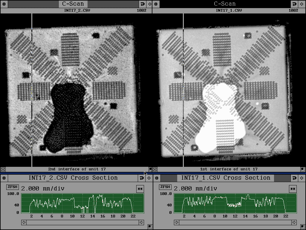
Three modes are used to display pulse echo information. In the A mode, the transducer is not x-y scanned, and the acoustic information is generated from a spot. In the B mode, the transducer is scanned along a line. A 2-dimensional image is generated in which one axis is the x-position of the transducer and the other axis is the time of flight for reflected pulses. The amplitude of the reflected pulse is mapped as intensity on the time of flight axis. Images created in the B-mode resemble cross-sections of samples. In the C-mode, the transducer is moved in a raster fashion. A 2-dimensional image is generated in which the x-y position in the image corresponds to an x-y position of the transducer. The intensity of a given x-y position on the image is proportional to the amplitude of the reflected signal at a given time of flight. Using this time window, a C-mode image can be generated to the extent of the flaw at a particular depth in the sample.
Acoustic Imaging, as used for microelectronic failure analysis, comprises three techniques that utilize ultrasonic imaging technology. The three acoustic microscopy technologies are the Scanning Laser Acoustic Microscope (SLAM), the Scanning Acoustic Microscope (SAM), and the C-Mode Scanning Acoustic Microscope (C-SAM). All three techniques are nondestructive.
The Scanning Laser Acoustic Microscope (SLAM) is a transmission microscope system that uses a transducer to generate an ultrasonic wave and a laser beam to detect the transmitted waves. Because ultrasonic waves attenuate rapidly in air, a liquid medium such as water or Flourinert™ is used to provide better acoustic transmission characteristics. As the acoustic waves propagate through the sample, voids and dissimilar interfaces will reduce the transmission of the acoustic waves. The laser detector on the back side of the sample then detects the waves as they hit the interface between the coverslip and the fluid couplant. Voids, dissimilar interfaces and other defects that alter the transmission properties of the acoustic waves can then be detected as regions of poor acoustic transmission. This signal can be turned into a map by scanning the laser detector.
The Scanning Acoustic Microscope (SAM) is a surface measurement system that looks at the reflected image from the surface of the sample. At very high acoustic frequencies, one can obtain an image of the surface to be examined similar to that of an optical image. This technique can also yield information about the elastic properties of the material. A complete image can be produced in approximately 10 seconds. This technique is not widely used for IC failure analysis.
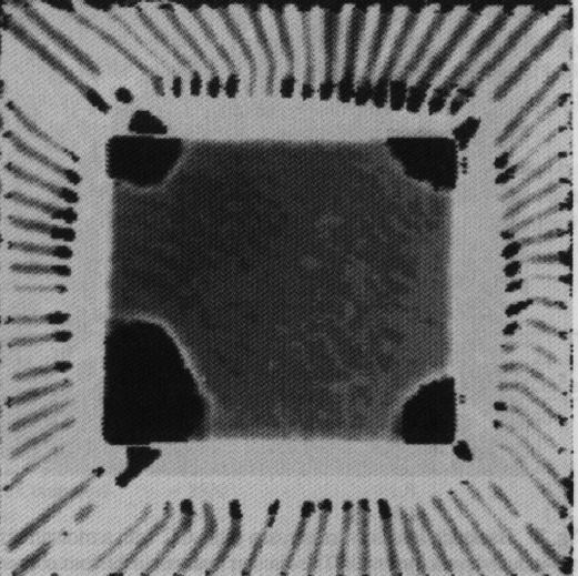
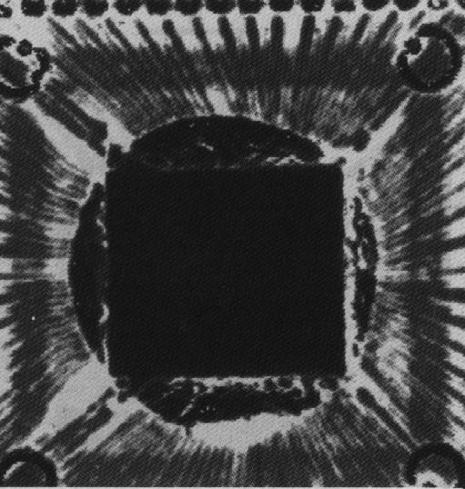
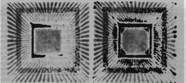
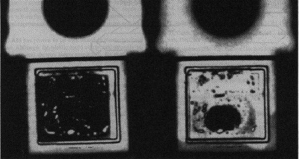
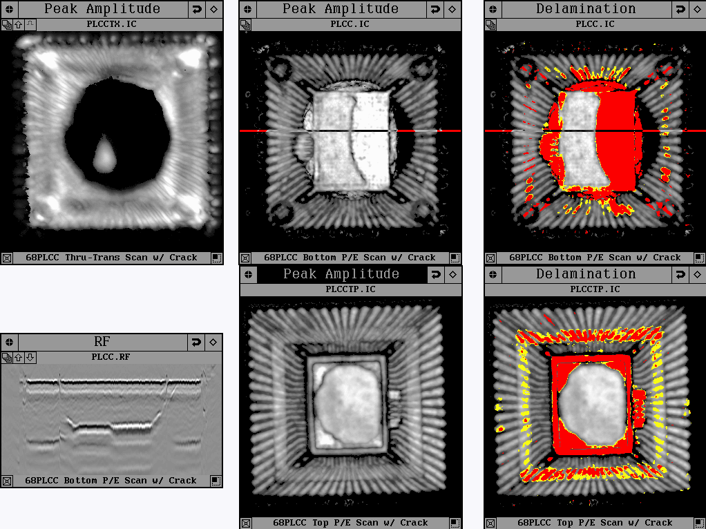
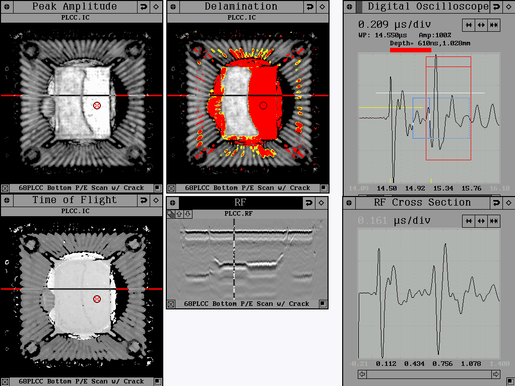
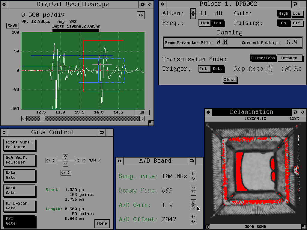
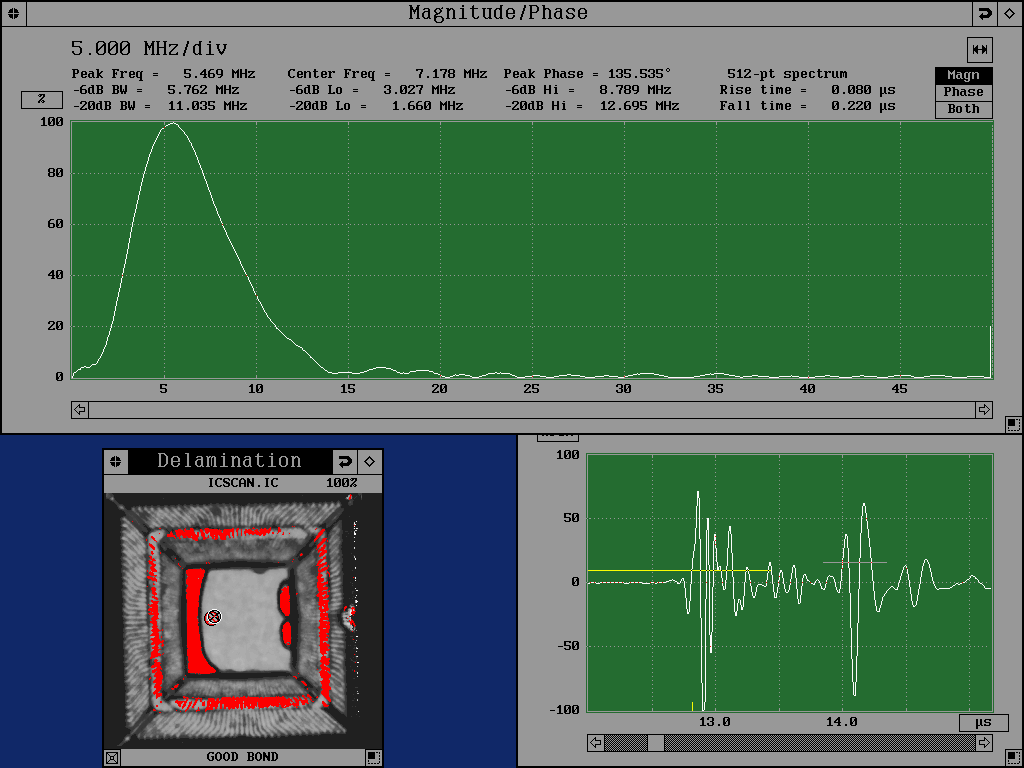
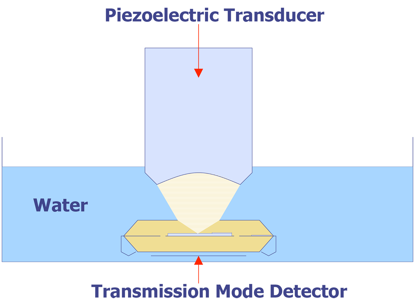
The C-Mode Scanning Acoustic Microscope (C-SAM) is an instrument that examines reflected waves from interfaces external and internal to the sample. The transducer acts as both the sender and receiver (see Figure 2). A very short acoustic pulse enters the sample and return echoes are produced at specific interfaces within the part (see Figure 3). The return times are a function of the distance from the interface from the interface to the transducer. This can be seen in Figure 4, where an echo from the initial interface shows up as a signal after about 0.5 microseconds, and the echo from an internal delamination shows up as a signal about 1 microsecond later.


An electronic gate can be set to examine a specific period of time corresponding to echoes from a particular interface. In the C-Mode of operation, the transducer can produce a map of the interface. This data contains information as to the quality of the interface within the package. This mode is most useful for examining delaminations, voids, and cracks, as well as die attach quality, in packaged ICs.
The lateral resolution (d) of a spherically focused probe for sub-surface inspection can be estimated by the following equation:


Here, λ is the acoustic wavelength, F is the focal length, and D is the diameter of the lens. Typically, the effective F/D ranges from 1 to 1.6 for plastic package inspection. At a center frequency of 20 MHz, the wavelength is approximately 170 ?m, and the calculated resolution is 270 ?m. This is an ideal resolution that does not account for attenuation. The observed resolution is roughly 400 ?m at a depth of 1.6 ?m (or 3.2 ?m round trip) in a standard PLCC package. Mold compound attenuation varies considerably from one formulation to the next and this dramatically affects the lateral resolution. Both the penetration and resolution are noticeably degraded by temperature shock damage to the molding compound.
The acoustic attenuation in mold compound has been reported to be 40 dB/cm at 15 MHz and increases rapidly with increasing frequency. The package preferentially attenuates the higher frequencies. As a result, acoustic inspections of standard PLCC packages are limited to roughly 20 MHz. However, thin plastic packages (mm) are often inspected at frequencies up to 90 MHz.
Attenuation also affects the depth resolution, especially in plastic package inspection. The decay period for a broad-band echo pulse is roughly 1.5l, which creates a "dead zone" after each reflection. In the "dead zone," later reflections cannot be temporarily resolved without the use of frequency domain analysis methods. This dead zone becomes thinner as the center frequency is increased.
In ceramic packages, the attenuation is much less (<.05 dB/cm), but the speed of sound is almost three times greater than that of mold compound. Hence, one wavelength at 50 MHz is Al2O3 is 200 mm and roughly equivalent to one wavelength in mold compound at 20 MHz. A lateral resolution approaching one wavelength is observed at a center frequency of 50 MHz and a depth of 1.6 mm in Al2O3.
The sensitivity of reflection acoustic imaging is superior to the lateral resolution of the technique. For example, 25 mm (1 mil) bond wires are often seen in 20 MHz C-SAM at 1.6 mm in plastic package inspections with an acoustic wavelength of 170 mm. A weakly reflecting object with lateral dimensions much larger than a wavelength that is easily detected in reflection may produce only a negligibly small contrast effect in transmission. However, the apparent size of a small, non-specular reflector in the image will be determined by the lateral resolution available.
The sensitivity of reflection mode acoustic imaging to thin cracks with lateral dimensions much larger than a wavelength is an important aspect of C-SAM inspection. Sound is a matter wave and depends on molecular vibration for propagation. Theory predicts that crack openings should be detectable if they are greater than the particle displacement amplitude produced by the interrogating sound wave. Experiments with steels, for example, indicate that air-filled cracks on the order of 10nm are detectable.
Other than acoustic impedance, the major variable of acoustic analysis is frequency. At higher frequencies, sensitivity in detecting small cavities is increased. Unfortunately, the maximum depth of useful information is reduced at higher frequencies. Normally, a compromise is needed to optimize sensitivity and sound beam penetration. For silicon IC examinations, frequencies of 30 to 50 MHz are used. This yields a maximum theoretical sensitivity of 20 microns; therefore, the depth of cavities and flaws cannot be located more accurately than 20 microns. The x-y resolution of acoustic microscopy depends upon a number of variables, including frequency, sample absorption, scattering, and the x-y scanning step size of the transducer.
| Material | velocity (m/sec) | density (g/cc) | Impedance (105g/cm2sec) |
|---|---|---|---|
| Al2O3 | 10400 | 3.8 | 40 |
| Cu | 4400 | 8.9 | 39 |
| Si | 8430 | 2.4 | 20 |
| Mold Compound | ~3500 | 1.8 | 6.3 |
| Water | 1480 | 1.0 | 1.5 |
| Air | 343 | 1.2x10⁻³ | 4.1x10⁻⁴ |


Acoustic Microscopy is a non-destructive test for locating delaminations, voids, and cracks in packaged ICs and examining die attach. Acoustic Microscopy can yield this information without the need for delidding the IC. Acoustic Imaging can also image voids and delaminations more easily than x-ray imaging can.
Acoustic Microscopy is performed using an ultrasonic piezoelectric transducer. The transducer sends out signals and the reflected signal is sensed with the piezoelectric material. Several manufacturers make commercial instruments for acoustic imaging of integrated circuits. The two biggest manufacturers of acoustic imaging equipment for integrated circuits are Sonoscan and Sonix. Both companies offer turn-key systems with easy-to-use software interfaces.
Acoustic Microscopy is normally performed before delidding the IC; however, if you need better spatial resolution while examining for voids or delaminations in the die attach, you can remove the lid to examine the IC.