Are you looking for more information regarding this and other subjects? Look no further than Semitracks' Online Training. Semitracks' Online Training contains short courses and other material useful for any Engineer trying to learn new subjects or brush up on old ones.
What is X-Ray Radiography?
X-ray Radiography involves the use of invisible, highly penetrating, short wavelength electromagnetic radiation to nondestructively obtain an image of hidden details of an IC device. This radiation is generated by an X-ray tube in laboratory equipment and transmitted through the sample of interest, where it is attenuated depending on density, structure and thickness of materials. Areas where more radiation is transmitted (light elements, thin sections) produce a higher signal or a darker area on the film. When the source of radiation is very small, magnification can be achieved with good resolution. Two techniques are commonly employed:
Conventional radiography makes use of transmitted radiation to expose film, which is developed using photographic techniques to reveal an image (see Figure 1). This is the more established technique, well-known for its medical applications, and laboratory equipment involved is relatively inexpensive.
Conventional X-ray Extended Source.
The real time technique involves the projection of an image as the part is being irradiated, which eliminates waiting time between exposure and evaluation, is amenable to image processing, and provides flexibility for maneuvering parts for views which convey the most information (see Figure 2). This technique involves more expensive equipment, but it is becoming increasingly accepted.
Microfocus X-Ray Source.
Approximate Equivalence Factors of Metals (after Colagelo). Note: Aluminum is the standard at 50 kV and 100kV, and steel at higher kV. (a) Tin or lead alloyed in brass increases these factors. (b) Numbers in parenthesis are estimates based on representative alloys.
Metal
Density, gm/cm3
Atomic Number
50kV
100kV
150kV
220kV
Magnesium
1.74
12
0.6
0.6
0.05
0.08
Aluminum
2.70
13
1.0
1.0
0.12
0.18
2024 Al Alloy
(2.99)b
(14)
1.4
1.2
0.13
0.14
Steel
(7.81)
(26)
12.0
1.0
1.0
Copper
8.96
29
18.0
1.6
1.4
Zinc
7.14
30
1.4
1.3
Brass(a)
(8.32)
(29)
1.3
1.3
Lead
11.4
82
14.0
12.0
Radiation Damage Threshold for Common Device Technologies (after Colangelo). Note: (a) Crystals will show part per million frequency shifts, although the effect is temporary and will anneal out.
Generic Technology
Damage Threshold, RAD (Si)
ECL, TTL, GaAs
200k to 10 Meg
Linear, I2L
15k to 1 Meg
MNOS, PMOS
8k to 100k
CMOS, VMOS, NMOS
0.8k to 10k
Quartz crystals (natural) (a)
100 to 1k
Why Perform an X-Ray Examination?
Early detection of a defect may change the course of subsequent failure analysis efforts. An X-ray examination frequently permits details of a particular failure to be discerned prior to or in lieu of any invasive or destructive procedure. It may also permit identification of a defect before it would otherwise be obscured by subsequent procedures. Many categories of defect can be resolved. Using the MIL-STD as a guide, the following conditions can be anticipated:
Sealing (solder)
Seal ring voiding, fillet defect, or incomplete melting.
Extraneous material (solder balls, etc.)
Die attach
Excessive voiding in attach medium.
Excessive bond material buildup.
Bonding material separated from main bond area.
Thickness gradient in bond material.
Bond Wires
Crossover or apparent contact of bond wires (Y, or top view).
Inadequate internal clearance of bond wires.
Excessive bond tail length.
Absence of arc in wire.
Sagging of wires.
Wire placement.
Bond spacing.
Other
Foreign material.
Excessive undercut at die edge.
Package post burrs.
Deviation from specified design or construction.
Circuit metallization pattern.
Cracks, splits or chips.
Unstated, obvious defects.
X-ray examination is neither effective as a replacement for a hermeticity test nor as a substitute for PIND testing, but it may complement either of these procedures. Certain features may remain hidden, such as aluminum wirebonds, nonconductive die attach media, semiconductor particles, or very fine details.
How is an X-Ray Examination Performed?
An X-ray tube is usually the source for X-ray equipment. In this evacuated glass bulb, electrons are emitted from a heated cathode and accelerated to several thousands of electron-volt levels, whereapon they strike a metal anode, producing X-rays.
Two types of X-ray examination are in use. The mil standard MIL-STD 883C, Method 2012.5, was originally written as a device screening procedure using radiography, but includes provisions for accepting real time (or non-film) techniques. The technique can be of use to the failure analyst without the strict compliance or certification to the MIL-STD, but familiarity with the mil standard will help the analyst make prudent decisions.
Radiography is the use of film to capture an X-ray image. The parts to be examined are usually placed directly on the film, which is in a light-tight envelope for handling and transportation. The part is irradiated in a suitable, safe enclosure in as many orientations as required. When the film is developed, the radiograph can be viewed with magnification or photographically reproduced.
"Real Time" techniques involve the use of a detector whose output is directed to a video display. Because the part is examined as it is being irrradiated, it can be translated or rotated by remote manipulators to achieve a perspective which gives the best information. Magnification, image quality and other factors can be optimized quickly. There is also a provision for a hardcopy of X-ray images on this type of equipment.
The X-rays must be energetic enough to penetrate the sample features of interest, but should not be so energetic as to cause damage. The MIL-STD limits voltages to a maximum of 150kV. Reference 1 tabulates radiation damage threshold doses for common device technologies. CMOS, VMOS, and NMOS structures are listed as the most sensitive, with thresholds from 0.8 kRAD (Si) to 10 kRAD (Si). A RAD is cited in Ref. 1 as "the absorbed dose of any ionizing radiation which is accompanied by the liberation of 0.01 joule of energy per kilogram of absorbing material."
When is an X-Ray Examination Performed?
X-ray examination can be performed on a lidded or encapsulated device prior to attempting to open or decapsulate the device. X-ray examination at this point minimizes foreign material, which may confuse the analysis.
PURPOSE. The purpose of this examination is to nondestructively detect defects within the sealed case, especially those resulting from the sealing process, and internal defects such as foreign objects, improper interconnecting wires, and voids in the die attach material or in the glass when glass seals are used. It establishes methods, criteria, and standards for radiographic examination of semiconductor devices.
NOTE: For certain case types, opacity of the construction materials (packages or internal) may effectively prevent radiographic identification of certain types of defects from some or all possible viewing angles. This factor should be considered in relation to the design of each device when application of this test method is specified.
APPARATUS. The apparatus and materials for this test shall include:
Radiographic equipment with a sufficient voltage range to penetrate the device. The focal distance shall be adequate to maintain a sharply defined image of an object with a major dimension of 0.0254 mm (0.001 inch).
Radiographic film: Very fine grain industrial X-ray film grade, either single or double emulsion.
Radiographic viewer: Capable of 0.0254 mm (0.001 inch) resolution in major dimension.
Holding fixtures: Capable of holding devices in the required positions without interfering with the accuracy or ease of image interpretation.
Radiographic quality standards: Capable of verifying the ability to detect all specified defects.
Film holder: A 1.6 mm (1/16 inch) minimum lead-topped table or lead-backed film holders to prevent back scatter of radiation.
PROCEDURE. The X-ray exposure factors, voltage, milliampere setting, and time settings shall be selected or adjusted as necessary to obtain satisfactory exposures and achieve maximum image details within the sensitivity requirements for the device or defect features the radiographic test is directed toward. The X-ray voltage shall be the lowest consistent with these requirements and shall not exceed 150 kV.
Mounting and views. The devices shall be mounted in the holding fixture so that the devices are not damaged or contaminated and are in the proper plane as specified. The devices may be mounted in any type of fixture and asking with lead diaphragms or barium clay may be employed to isolate multiple specimens provided the fixtures or masking materials do not block the view from X-ray source to the film of any portion of the body of the device.
Views.
Flat packages, dual-in-line packages, and single ended cylindrical devices, unless otherwise specified, shall have one view taken with the X-rays penetrating in the Y direction as defined in Figure 1 and Figure 2 of MIL-STD-883, GENERAL REQUIREMENTS. When more than one view is required, the second and third views, as applicable, shall be taken with the X-rays penetrating in the Z and X direction respectively (either Z or X for flat packages). Position the die/cavity interface as close as possible to the film to avoid distortion.
Stud-mounted and cylindrical axial lead devices, unless otherwise specified, shall have one view taken with the X-rays penetrating in the X direction as defined in Figure 1 and Figure 2 of MIL-STD-883, GENERAL REQUIREMENTS. When more than one view is required, the second and third views, as applicable, shall be taken with the X-rays penetrating in the direction and at 45 degrees between the X and Z direction. Position the die/cavity interface as close as possible to the film to avoid distortion.
Radiographic quality standard. Eachradiograph shall have at least two quality standards exposed with each view located (and properly identified in opposite corners of the film. These penetrameters shall be of a radiographic density nearest the density of the devices being inspected. The radiographic quality standard shall consist of a suitable ASTM penetrameter as described in the DoD adopted standard ASTM E 801-81a, Standard Practice For Controlling Quality of Radiographic Testing of Electronic Devices, or equivalent.
Film and marking. The radiographic film shall be in a film holder backed with a minimum of 1/16 inch lead or the holder shall be placed on the lead-topped table. The film shall be identified using techniques that print the following information, photographically, on the radiograph:
Device manufacturer's name or code identification number.
Device type or part number.
Production lot number or date code or inspection lot number.
Radiographic film view number and date.
Device serial or cross reference numbers, when applicable.
X-ray laboratory identification, if other than device manufacturer.
Nonfilm techniques, when specified. The use of nonfilm techniques is permitted if permanent records are not required and the equipment is capable of producing results of equal quality when compared with film techniques, and all requirements of this method are complied with, except those pertaining to the actual film.
Serialized devices. When device serialization is required, each device shall be readily identified by a serial number. They shall be radiographed in consecutive, increasing serial order. When a device is missing, the blank space shall contain either the serial number or other X-ray opaque to readily identify and correlate X-ray data. When large skips occur within serialized devices, the serial number of the last device before the skip and the first device after the skip may be used in place of the multiple opaque objects.
Special device marking. When specified (see 4.c), the devices that have been X-rayed and found acceptable shall be identified with a blue dot on the external case. The blue dot shall be approximately 1/16 inch in diameter. The color selected from FED-STD-595 shall be any shade between 15102-15123 or 25102-25109. The dot shall be placed so that it is readily visible but shall not obliterate other device marking.
Tests. The X-ray exposure factor shall be selected to achieve resolution of 0.0254 mm (0.001 inch) major dimension, less than 10 percent distortion and an "H" and "D" film density between 1 and 2 in the area of interest of the device image. radiographs shall be made for each view required (see 4).
Processing. The radiographic film manufacturer's recommended procedure shall be used to develop the exposed film, and film shall be processed so that it is free of processing defects such as fingerprints, scratches, fogging, chemical spots, blemishes, etc.
Operating personnel. Personnel who will perform radiographic inspection shall have training in radiographic procedures and techniques so that defects revealed by this method can be validly interpreted and compared with applicable standards. The following minimum vision requirements shall apply for visual acuity of personnel inspecting film:
Distant vision shall equal at least 20/30 in both eyes, corrected or uncorrected.
Near vision shall be such that the operator can read Jaeger type No. 2 at a distance of 16 inches, corrected or uncorrected.
Vision tests shall be performed by an oculist, optometrist, or other professionally recognized personnel at least once a year. Personnel authorized to conduct radiographic tests shall be required to pass the vision ests specified in 3.6 a and b.
Interpretation of radiographs. Utilizing the equipment specified herein, radiographs shall be inspected to determine that each device conforms to this standard and defective devices shall be rejected. Interpretation of the radiograph shall be made under low light level conditions without glare on the radiographic viewing surface. The radiographs shall be examined on a suitable illuminator with variable intensity or on a viewer suitable for radiographic inspection on projection type viewing equipment. The radiograph shall be viewed at a magnification between 6X and 25X. Viewing masks may be used when necessary. Any radiograph not clearly illustrating the features in the radiographic quality standards is not-acceptable and another radiograph of the devices shall be taken.
Reports of records.
Reports of inspection. For class S devices, or when specified for other device classes, the manufacturer shall furnish inspection reports with each shipment of devices. The report shall describe the results of the radiographic inspection, and list the purchase order number or equivalent identification, the part number, the date code, the quantity inspected, the quantity rejected, and the date of test. For each rejected device, the part number, the serial number, when applicable, and the cause for rejection shall be listed.
Radiograph submission. Photographic eproduction of complete radiographs may be submitted, but art portions are not acceptable.
Radiograph and report retention. When specified, the manufacturer shall retain a set of the radiographs and a copy of the inspection report. These shall be retained for the period specified.
Examination and acceptance criteria.
Device construction. Acceptable devices shall be of the specified design and construction with regard to the characteristic discernible through radiographic examination. Devices that deviate significantly from the specified construction shall be rejected.
Individual device defects. The individual device examination shall include, but not be limited to, inspection for foreign particles, solder or weld "splash" build up of bonding material, proper shape and placement of lead wires or whiskers, bond of lead or whisker to semiconductor element and lead or whisker to terminal post, semiconductor metallization pattern, and mounting of semiconductor element. Any device for which the radiograph reveals any of the following defects shall be rejected.
Presence of extraneous matter. Extraneous matter (foreign particles) shall include, but not be limited to:
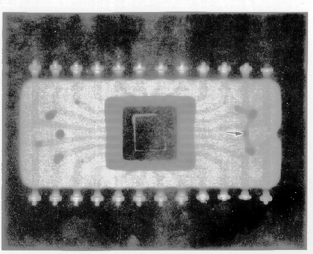
Any foreign particle, loose or attached, greater than 0.025 mm (0.001 inch) (see Figure 6), or of any lesser size which is sufficient to bridge nonconnected conducting elements of the device.
Any wire tail extending beyond its normal end by more than two diameters at the semiconductor die pad or by more than four wire diameters at the package post (see Figure 6).
Any burr on a post (header lead) greater than 0.08 mm (0.003 inch) in its major dimension or of such configuration that it may break away.
Excessive semiconductor element bonding material buildup.
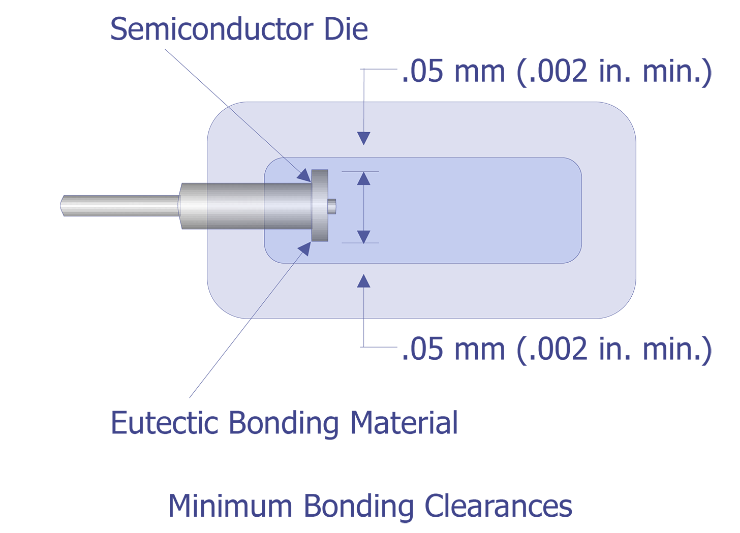
A semiconductor element shall be mounted and bonded so that it is not tilted more than 10 degrees from the normal mounting surface. The bonding agent that accumulates around the perimeter of the semiconductor element and touches the side of the semiconductor element shall not accumulate to a thickness greater than the height of the semiconductor element (see Figure 7 and Figure 8). Where the bonding agent is built up but is not touching the semiconductor element, the buildup shall not be greater than twice the height of the semiconductor element, or any lead or post, or separated from the main bonding material area (see Figure 21).
There shall be no visible extraneous material 0.025 mm (0.001 inch) or larger in the major dimension. Loose bonding material will be considered extraneous material. Excessive (but not loose) bonding material will not be considered extraneous unless it fails to meet the requirements of 3.9.2.1.d.1 or unless the accumulation of bonding material is such that the height of the accumulation is greater than the width of its base or that the accumulation necks down at any point (see Figure 7 and Figure 8).
Gold flaking on the header or posts or anywhere inside the case.
Extraneous ball bonds anywhere inside case, except for attached bond residue when bonding is allowed.
Unacceptable construction. In the examination of devices, the following aspects shall be considered unacceptable construction and devices that exhibit any of the following defects shall be rejected:
Voids - When radiographing devices, certain types of mounting do not give true representations of voids. When such devices are inspected, the mounting shall be noted on the inspection report (see Figure 6).
Contact area voids in excess of one-half of the total contact area.
A single void which traverses either the length or width of the semiconductor element and exceeds 10 percent of the total intended contact area.
Wires present, other than those connecting specific areas of the semiconductor element to the external leads. Device designs calling for the use of such wires including jumper wires necessary to trim load resistors are acceptable (see Figure 6).
Cracks, splits, or chips of the electrical elements.
Excessive undercutting of the electrical elements (X and Z plane only, see Figure 9).
Defective seal - Any device wherein the integral lid seal is not continuous or is reduced from its designed sealing width by more than 75 percent. Expulsion resulting from the final sealing operation is not considered extraneous material as long as it can be established that it is continuous, uniform and attached to the parent material and does not exhibit a ball, splash or tear-drop configuration (i.e., where the base support least dimension is smaller than the dimension it is supposed to support).
Inadequate clearance - Acceptable devices shall have adequate internal clearance to assure that the elements cannot contact one another or the case. No crossover shall be allowed. Depending upon the case type, devices shall be rejected for the following conditions:
Any lead wire that appears to touch or cross another lead wire or bond (Y plane only).
Any lead wire that deviates from a straight line from bond to external lead and appears to be within 0.05 mm (0.002 inch) of another bond (Y plane only).
Lead wires that do not deviate from a straight line from bond to external lead and appear to touch another wire or bond (Y plane only).
Any lead wire that touches or comes within 0.05 mm (0.002 inch) of the case or external lead to which it is not attached (X and Y plane).
Any bond that is less than 0.025 mm (0.001 inch) (excluding bonds connected by a common conductor) from another bond (Y plane only).
Any wire making a straight line run from die bonding pad to package post that has no arc.
Lead wires that sag below an imaginary plane across the top of the die bond (X plane only) except by design.
Any lead wire that touches or comes within 0.05 mm (0.002 inch) of the case or external lead to which it is not attached (X and Y plane).
Lead wires that sag below an imaginary plane across the top of the die bond (X plane only) except by design.
Any lead wire that appears to touch or cross another lead wire or bond (Y plane only).
Any lead wire that deviates from a straight line from bond to external lead and appears to touch or to be within 0.05 mm (0.002 inch) of another wire or bond (Y plane only).
Any bond that is less than 0.025 mm (0.001 inch) (excluding bonds connected by a common conductor) from another bond (Y plane only).
Any wire making a straight line run from die bonding pad to package post that has no arc, unless specifically designed in this manner (e.g., clips or rigid connecting leads).
Any internal post that is bent more than 10 degrees from the vertical (or intended design position) or is not uniform in length and construction or comes closer than one post diameter to another post.
Where a low profile case (such as a T0-46) is used, any post which comes closer to the top of the case than 20 percent of the total inside dimension between the header and the top of the case. In devices which have the semiconductor element vertical to the header, any device where the semiconductor element comes closer than 0.05 mm (0.002 inch) to the header or to any part of the case.
Any case which does not have a header design incorporating a header edge or other feature (e.g., a "splash ring") to prevent solder or weld splash from entering the interior of the case.
Whisker-to-case distance less than one-half the diameter of the external lead wire.
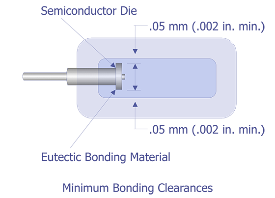
Distance from case to semiconductor die or to any eutectic bonding material less than 0.05 mm (0.002 inch).
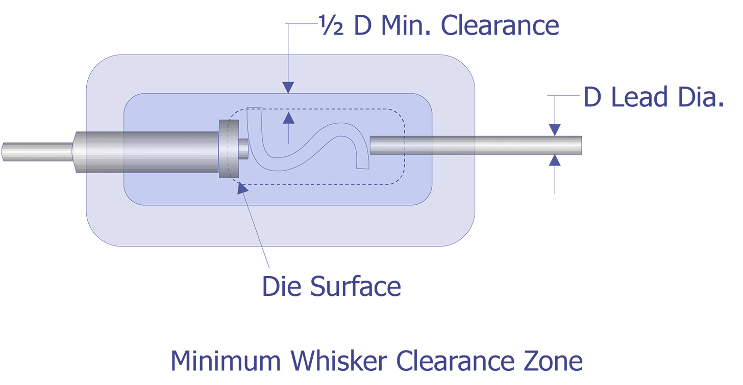
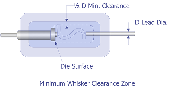
Whisker tilted more than 5 degrees in any direction from the device lead axis or deformed to the extent that it touches itself.
C- and S-shaped whisker with air gap between any two points on it less than twice the diameter or thickness of the whisker wire. On diodes with whiskers metallurgically bonded to the post and to the die, the whisker may be deformed to the extent that it touches itself if the minimum whisker clearance zone specified in Figure 22 is maintained.
Whiskerless construction device with anode and cathode lead connections displaced more than 0.25 mm (0.01 inch) with respect to the central axis of the device.
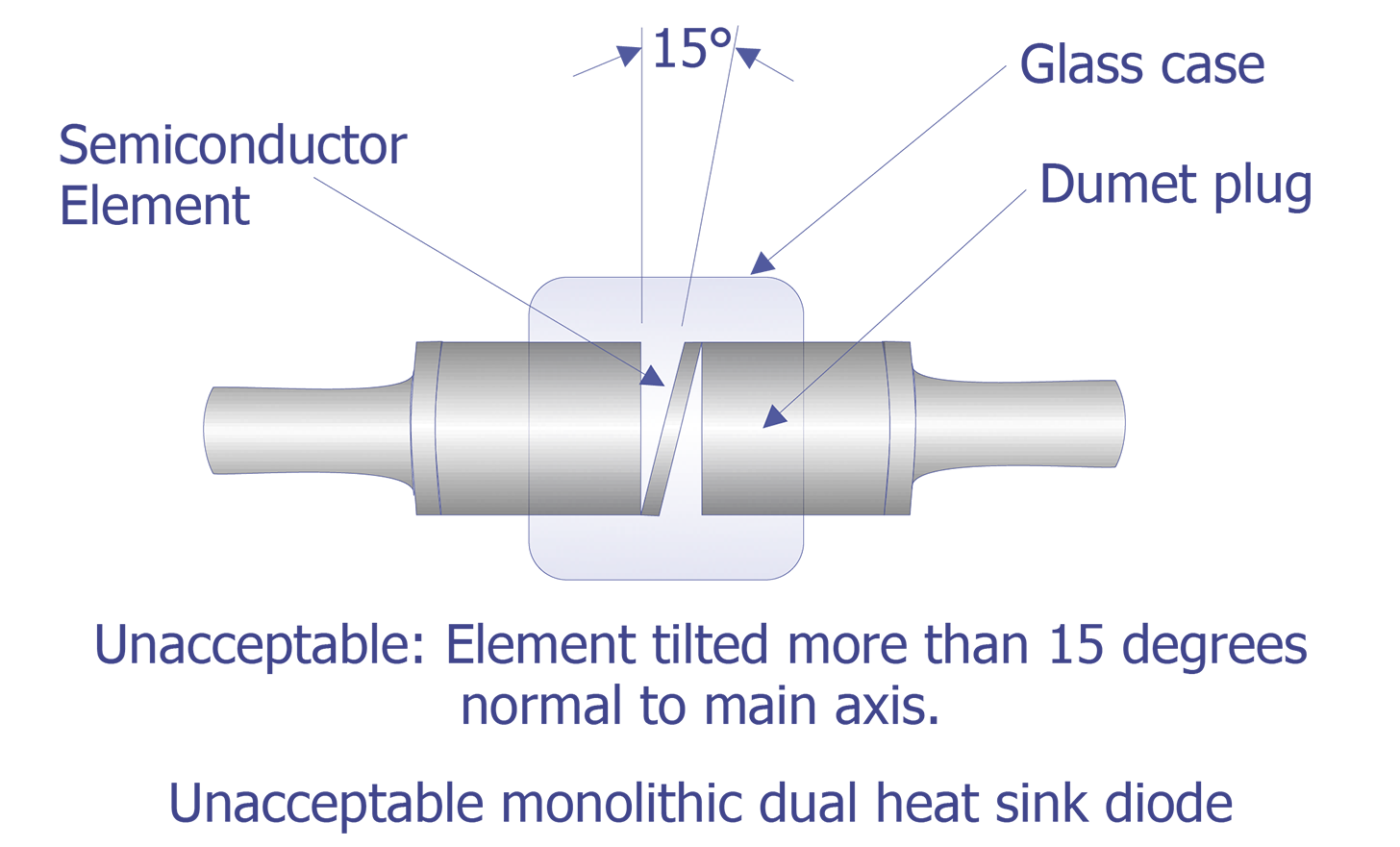
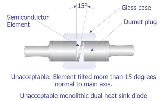
Semiconductor element mounting tilted more than 15 degrees from normal to the main axis o the device.
Die hanging over edge of header or pedestal more than 10 percent of the die area.
Less than 75 percent of the semiconductor element base area is bonded to the mounting surface.
Voids in the welds, from any edge, between the leads and the heat sink slugs greater than 15 percent of the lead wire diameter. Any voids whatever in the central part of the area that should be welded.
Devices with package deformities such as, body glass cracks incomplete seals (voids, position of glass, etc.,), die chip outs and severe misalignment of S- and C-shaped whisker connections to die or post.
SUMMARY. The following details shall be specified in the applicable procurement document:
Number of views, if other than indicated in 3.1.1.
Radiograph submission, if applicable (see 3.8.2).
Marking, if other than indicated in 3.3 and marking of samples to indicate they have been radiographed, if required (see 3.3.3).
Defects to be sought in the samples and criteria for acceptance or rejection, if other than indicated in 3.9.
Radiograph and report retention, if applicable (see 3.8.3).
Test reports when required for class B or C devices.
References on X-Ray Examination
Advanced Radiographic Techniques in Failure Analysis, Joe Colangelo, Microelectronic Failure Analysis, Desk Reference, 3rd Edition, Ed. Thomas W. Lee and Seshu V. Pabbisetty, ASM International, 1993, pp. 51-58.
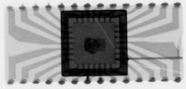
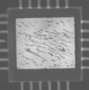
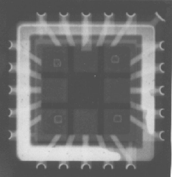
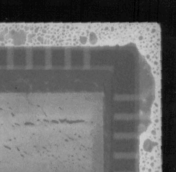
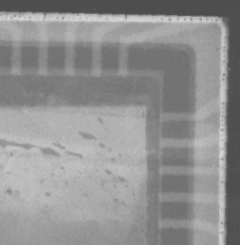
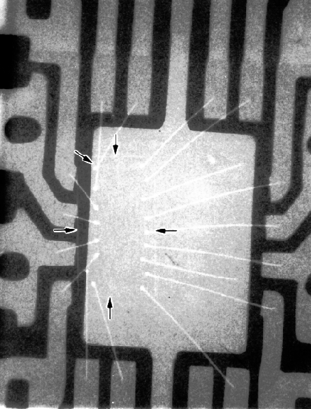
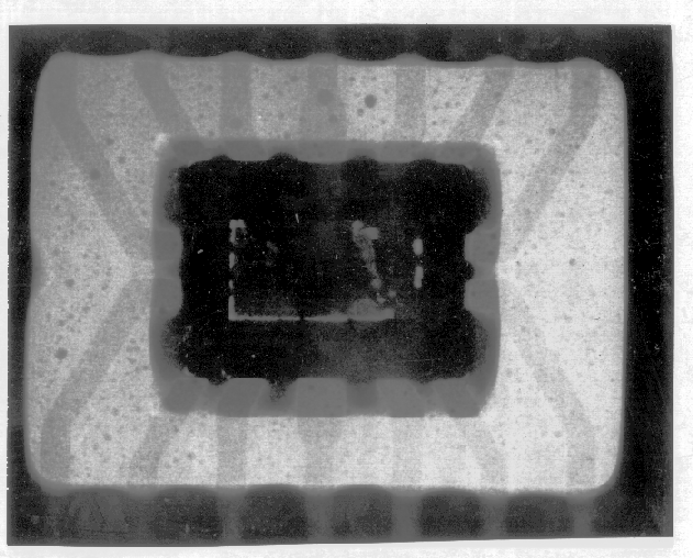
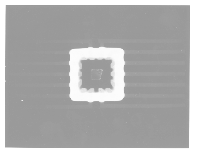
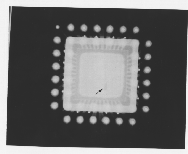
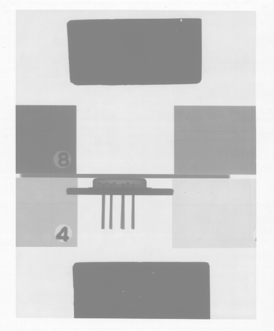
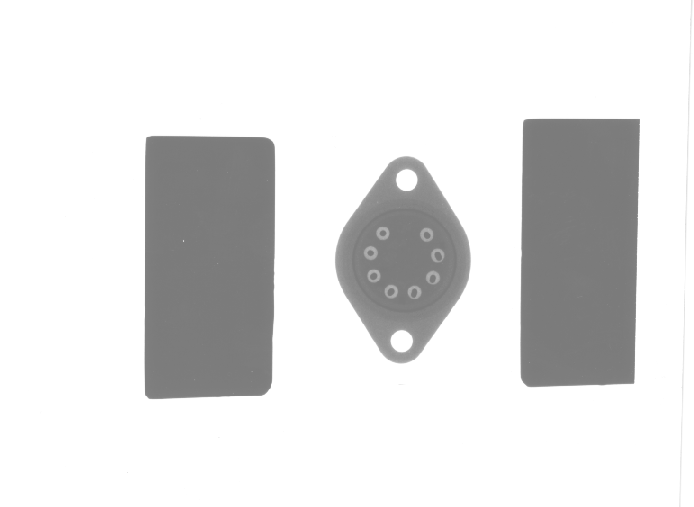
Figure 1. X-ray image showing a Dual In-line Package (DIP) which has a crack running through the ceramic body. This radiograph was produced on a positive acting Polaroid print medium. (Courtesy Sandia Labs).Figure 2. X-ray image showing an enlargement of a portion of a package cavity, showing directional voiding occurring in a silicon-gold eutectic die attach process. This radiograph was produced on fine grained Xray film and reproduced by backlighting and photographing the negative. (Courtesy Sandia Labs).Figure 3. X-ray image showing a Leadless Chip Carrier (LCC) which had a ceramic lid sealed to it using gold-tin eutectic solder in a heated platen sealer. The defect in the lower left corner resulted from a raised corner on the lid which caused a breach in the solder seal. (Courtesy Sandia Labs).Figure 4. X-ray image showing a very porous and poorly wetted seal ring following lid sealing. Note that die attach detail is also revealed. (Courtesy Sandia Labs).Figure 5. X-ray image showing porosity evident in the fillet region of a ceramic package sealed with a metal lid. This porosity was not typical, and indicated a material problem. (Courtesy Sandia Labs).Figure 6.Figure 7.Figure 8.Figure 9.Figure 10.Figure 11.Figure 12.Figure 13.Figure 14.Figure 15.Figure 16.Figure 17.Figure 18.Figure 19.Figure 20.Figure 21.Figure 22.Figure 23.Figure 24.Figure 25.Figure 26.Figure 27.Figure 28.


